Active production — what the 5000Vrms and 6A peak mean for a gate-drive BOM
The SI823H3AD-IS3 is an active-production single-channel digital isolator from Skyworks' Si823Hx family, built on capacitive coupling technology. It delivers 5000Vrms of galvanic isolation — enough to separate the low-voltage controller side from a high-side gate drive in a motor inverter or power supply, with the isolation barrier certified to CQC, CSA, UL, and VDE. The 6A peak output current drives the gate capacitance of a large IGBT or SiC MOSFET through the Miller plateau without excessive switching loss. The 4A source, 4A sink rating is the continuous drive capability; the 6A peak handles the initial charge injection into the gate during the turn-on transient.
125kV/µs CMTI and 116ns propagation delay — the switching margin numbers
Common-mode transient immunity of 125kV/µs minimum means the output state does not glitch when the high-side switch node slews at that rate — critical in a half-bridge where the floating ground jumps from 0V to the DC bus voltage in tens of nanoseconds. If the CMTI is too low for the application's dv/dt, the isolator's output can momentarily toggle, causing a shoot-through event. Propagation delay is 116ns max from input to output, symmetrical within 5ns pulse-width distortion. This symmetry matters for dead-time insertion: if the turn-on and turn-off delays differ by more than the programmed dead band, the complementary switch can cross-conduct. Rise and fall times are 12ns typical (12ns max) into the rated load — fast enough to keep the switching transition inside the dead-time window but not so fast that the gate ringing couples back through the Miller capacitance. The 5.5V to 30V output supply range lets the gate drive voltage match the power device's threshold (typically 12V for IGBTs, 15V to 20V for SiC MOSFETs).
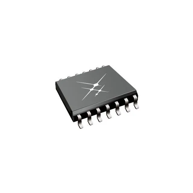
The 8mm creepage distance across the body meets the 5000Vrms reinforced isolation requirement per IEC 60747-17 — the wide SOIC is the standard package for this isolation class. The 14-SOIC's exposed pad (if present on the specific variant) should be soldered to a PCB copper island for thermal relief — the datasheet's recommended land pattern dictates the pad size.