Propagation delay and common-mode transient immunity — what they mean for switching
The SI8235AB-D-IS1R: Maximum propagation delay is 60 ns in both directions — the time from the logic input edge to the gate-drive output edge. In a 20 kHz PWM cycle (50 µs period), 60 ns is 0.12 % of the period, so the delay adds negligible dead-time error in most inverter designs. Common-mode transient immunity is a minimum of 20 kV/µs — the isolator does not latch or glitch when the output-side ground bounces relative to the input-side ground at that slew rate. This matters in half-bridge topologies where the high-side switch's source swings from ground to the DC bus in tens of nanoseconds. Pulse-width distortion is capped at 5.6 ns — the difference in delay between rising and falling edges stays below that figure, so the output duty cycle closely mirrors the input duty cycle without calibration.
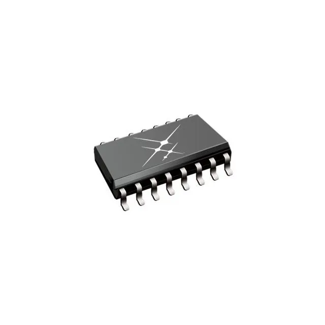
Package and supply rails — 16-SOIC footprint with 6.5 V to 24 V output supply
The output-side supply voltage range is 6.5 V to 24 V — covers the typical gate-drive rails for Si MOSFETs (10-15 V) and IGBTs (15-20 V) from a single part. The input-side supply is not separately specified in this listing, but the dual-channel architecture implies the input side draws from the controller's logic rail. Approvals include CQC, CSA, UR, and VDE — the part carries the safety-agency marks needed for UL 60950-1 and IEC 62368-1 end-equipment certification in industrial and automotive power supplies.
Active production — tape-and-reel packaging
The tube-packaged sibling SI8235AB-D-IS1 uses the same die and parametric profile.