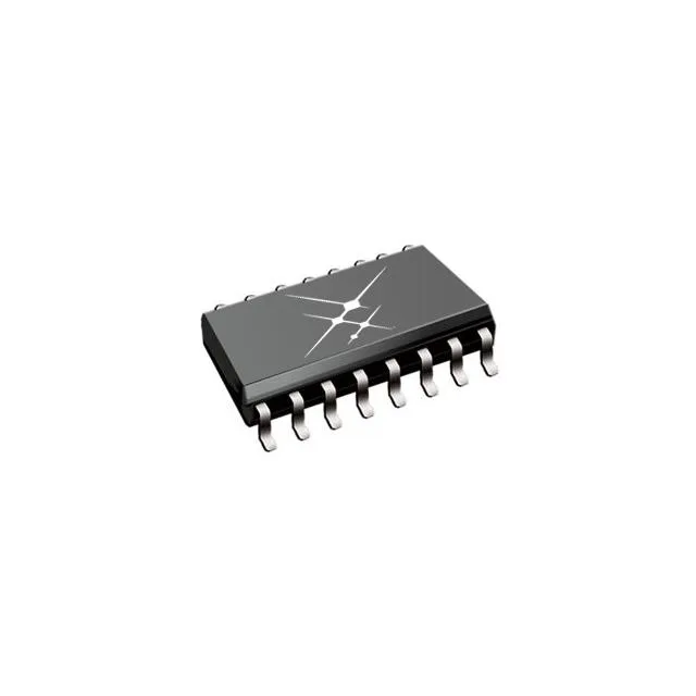
AEC-Q100 qualification and the under-hood temperature profile
The SI8233BB-D-IS1: This means the isolator's silicon and package are characterized for the full under-hood ambient profile — no derating required at the 105°C soak that an engine-bay ECU sees on a summer grade. The qualification covers the reliability stress tests (preconditioning, temperature cycling, HAST, high-temperature operating life) that tier-one automotive programs require for PPAP submission. A missing AEC-Q100 cert is a common gate for ECU release; this part clears it.
Isolation barrier and transient immunity for motor-drive gate drive
Rated for 2500Vrms isolation with a minimum common-mode transient immunity of 20kV/µs. In a motor-drive or inverter application, the high-side gate driver reference swings at the switching node — the CMTI figure tells you the isolator's internal coupling capacitance can reject that dv/dt without corrupting the output state. 20kV/µs is sufficient for most IGBT and SiC gate-drive circuits switching at 10-20 kHz. The isolation technology is capacitive coupling using SiO2 dielectric — no magnetic core or LED aging curve to budget. Capacitive isolators typically show lower propagation delay and tighter pulse-width distortion than optocouplers or magnetic isolators at equivalent voltage ratings.
Output drive strength and timing — what the 4A peak means for gate charge
Peak output current is 4A, with asymmetric source/sink: 2A source (high-side FET turn-on) and 4A sink (turn-off). The higher sink current pulls the gate down faster, which is the critical edge for dead-time management — a slow turn-off risks shoot-through in a half-bridge. For a typical 10 nC gate charge, the 4A sink discharges it in roughly 2.5 ns, though the package and PCB parasitics will dominate the actual fall time. Propagation delay is 60ns max (both tpLH and tpHL), with pulse-width distortion held to 5.6ns max. In a dead-time calculation, the 5.6ns PWD is the mismatch between the turn-on and turn-off propagation paths — budget it into the dead-time guard band so the complementary switch never sees both gates high simultaneously. Rise and fall times are 12ns typical, 12ns max — the output edge rate is fast enough to drive the gate of a power MOSFET without excessive switching loss, but the PCB layout must keep the gate-drive loop inductance below 10 nH to avoid ringing on the gate waveform.
Package, supply rails, and approvals for global BOM acceptance
Housed in a 16-SOIC narrow-body package (3.90mm body width), the same footprint used by most dual-channel digital isolators and gate drivers. The output supply range is 9.4V to 24V, covering the standard gate-drive rails for Si MOSFETs (12V) and IGBTs (15V) with margin. Approved by CQC (China), CSA (Canada), UR (UL-recognized, US), and VDE (Germany) — the four agencies that cover the major global markets for industrial and automotive equipment. No additional safety certification is needed for a BOM destined for multi-region production. RoHS3 compliant per — no exemption claims to track; the part ships with full material declaration for EU and China RoHS filing.