2.5A peak drive with 30kV/µs CMTI for inverter stages
The SI8220CB-D-IS: The output stage delivers 2.5A peak source/sink current, with a high-level drive of 1.5A and a low-level drive of 2.5A. This is sufficient to directly switch the gate capacitance of medium-power IGBTs and SiC MOSFETs in motor-drive or DC-DC converter stages without a separate booster buffer. Propagation delay is 60ns max (low-to-high) and 40ns max (high-to-low), while the common-mode transient immunity is a minimum of 30kV/µs. These two specs together mean the part maintains timing integrity and rejects fast common-mode noise edges — the kind generated by hard-switching inverter bridges — keeping the gate signal clean and preventing false turn-ons. The output supply range of 12.2V to 24V covers the typical gate-drive bias voltage for SiC MOSFETs (18-20V) and IGBTs (15V), and the 20ns typical rise/fall time keeps switching losses in the power device manageable at moderate frequencies.
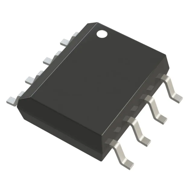
Board-fit: 8-SOIC narrow body, standard layout
The 8-SOIC narrow-body package (3.90mm width) is a common footprint shared by many isolated gate drivers and digital isolators. The surface-mount solder pads follow the standard SOIC-8 land pattern, with no exposed thermal pad — the part dissipates through the leads and the board copper. The tube packaging is typical for prototype and low-to-medium volume builds.