50 MHz HCS12X — what the core clock buys the design
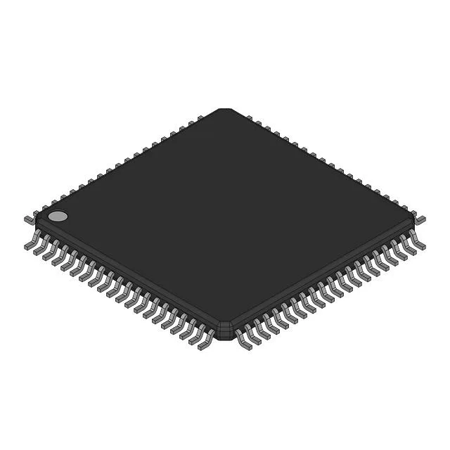
The NXP S912XES384J3CAA is a 16-bit HCS12X MCU clocked at 50 MHz, with 384 KB of on-chip Flash and 12-channel 12-bit SAR ADC. It's built for deterministic control loops—CANbus, SCI, SPI, and I2C all on the same die—so a single chip handles the gateway, sensor fusion, and actuator drive in an industrial controller or automotive body module. The 59 I/O lines and external bus interface (EBI/EMI) leave room for memory expansion or parallel peripherals without a CPLD.
384 KB Flash and 16-bit datapath — firmware headroom
384 KB of program Flash is generous for a 16-bit MCU in this class—enough for a CANopen stack, several PID loops, and a bootloader with OTA staging. The HCS12X core's single-cycle multiply and XGATE co-processor offload interrupt-heavy tasks, so the main loop doesn't stall on CAN message handling. If your firmware footprint is already pushing 256 KB, this part gives breathing room without a die-shrink migration.
CANbus, SCI, SPI — connectivity set for body control and industrial gateway
The S912XES384J3CAA includes CANbus, SCI (UART), SPI, and I2C, plus an IrDA module. In a typical automotive body controller, CAN handles the vehicle network, SCI talks to a Bluetooth module or debug port, and SPI drives an external CAN transceiver or sensor hub. The EBI/EMI interface lets you attach an external SRAM or FRAM without bit-banging GPIO—useful for data logging in motor-drive applications.
The operating supply range is 1.72 V nominal, which means a single 1.8 V rail can power the core and I/O, simplifying the power tree.
Listed as Active by NXP—no EOL notice, no LTB window.