RF power LDMOS for 512 MHz band
The NXP MRFE6VS25GNR1 is an LDMOS RF power transistor designed for 512 MHz operation, delivering 25 W output with 25.4 dB gain at a 50 V test supply. The 133 V rated drain-source breakdown gives headroom for load mismatch and high-VSWR conditions common in RF power amplifier output stages. The 10 mA test current is typical for small-signal gain characterization; actual bias current in class-AB operation will be higher.
The 133 V rated voltage means the device can survive transient overvoltage events up to that peak without avalanche failure, provided the thermal limit is respected. This is a ruggedness spec, not a continuous operating point.
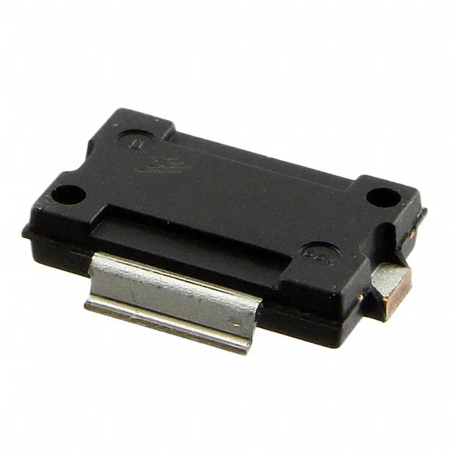
Package and mounting — TO-270-2 GULL
The TO-270-2 GULL surface-mount package has two gull-wing leads plus a large source tab on the bottom. The package footprint is smaller than a flanged bolt-down TO-272, saving board area in dense PA arrays. Cut Tape (CT) and Tape & Reel (TR) options are available for different assembly volumes. The surface-mount format suits automated pick-and-place lines, though the large tab may need a longer reflow profile for complete solder wetting.
No end-of-life notification or last-time-buy window has been published. This is a current-design-in part for new RF power amplifier projects, not a phase-out risk.