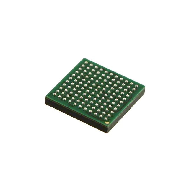
NXP Semiconductors MK51DX256CMC7 — Analog & Data Acquisition

NXP MK51DX256CMC7 Kinetis K50 MCU, ARM Cortex-M4, 72 MHz

MPNMK51DX256CMC7
End of Life

NXP Kinetis K50 MK51DX256CMC7, 32-bit ARM Cortex-M4 MCU, 72 MHz, 256 KB Flash, 64 KB RAM, 2 KB EEPROM, 35x16-bit ADC, 1x12-bit DAC, USB OTG, 121-MAPBGA (8x8 mm), -40°C to 85°C.

$17.49Ref. price · indicative, final on quote
Packaging121-LFBGA
StockContact for availability
MOQ1 pcs
  • 100% new & originalTraceable channels only — no refurbs, no pulls, no remarked parts.
  • Date & lot codes on quoteStated per line before you commit; label photos on request.
  • MSL-compliant ESD packingMoisture-sealed bags with indicator cards; reels photo-verified.
  • PayPal buyer protectionPay by T/T, PayPal or Payoneer — card payments covered end to end.

Specifications

MK51DX256CMC7 Technical Specifications
ParameterValue
SeriesKinetis K50
Mounting typeSurface Mount
Oscillator typeInternal
Program memory typeFLASH
Voltage - supply (Vcc (Vdd))1.71V ~ 3.6V
Operating temperature-40°C ~ 85°C (TA)
Speed72MHz
PackageTray
RAM size64K x 8
Core size32-Bit Single-Core
EEPROM size2K x 8
PeripheralsDMA, I²S, LVD, POR, PWM, WDT
ConnectivityI²C, IrDA, SPI, UART/USART, USB, USB OTG
Number of i (O)78
Core processorARM® Cortex®-M4
Case121-LFBGA
Data convertersA/D 35x16b; D/A 1x12b
Program memory size256KB (256K x 8)

Product details

72 MHz Cortex-M4 with 16-bit ADC array — the mixed-signal MCU for sensor-heavy designs

The MK51DX256CMC7: The core runs at 72 MHz with a single-cycle multiply and hardware divide, plus a single-precision FPU that offloads filter coefficients and sensor linearization from the main loop. Program memory is 256 KB of Flash, backed by 64 KB of SRAM and a separate 2 KB EEPROM block for configuration parameters that survive reprogramming cycles. The 35-channel 16-bit ADC is the standout peripheral — enough resolution and channel count to sample multiple analog sensors without an external multiplexer, while the single 12-bit DAC handles analog output or waveform generation. Connectivity includes USB with OTG, multiple I²C and SPI buses, UARTs with IrDA support, and an I²S audio interface. The 78 GPIOs in the 121-MAPBGA package give enough headroom for a sensor array plus a display or keypad. The internal oscillator reduces external BOM count, though a crystal can be added for tighter timing accuracy.

121-MAPBGA footprint — layout notes for the 8x8 mm array

The 121-MAPBGA (8x8 mm) package is a ball grid array. Decouple with a ceramic capacitor on the main rail and a capacitor per supply pin pair, placed as close to the balls as via geometry allows. The package is MSL 3 per the standard Kinetis BGA family — bake before reflow if the moisture barrier bag has been open longer than the floor-life window. No exposed thermal pad; junction temperature is managed through the BGA balls and the PCB copper plane. A four-layer board with a solid ground plane under the package is recommended for thermal and signal-integrity reasons.

ROHS3 compliant — no exemption-driven lead content.

Frequently asked questions

What is the price of MK51DX256CMC7?

Sourcing buyers need to compare pricing across distributors for BOM cost estimation.

What is the pinout of MK51DX256CMC7?

Design engineers need pin mapping for PCB layout and peripheral connection validation.

Is MK51DX256CMC7 obsolete?

Brokers and buyers need lifecycle status to avoid supply chain disruptions or redesigns.

What distributors carry MK51DX256CMC7?

Buyers need to know authorized sources for genuine parts and availability.

What is the alternative for MK51DX256CMC7?

Engineers may need a pin-compatible or functionally equivalent MCU if this part is unavailable or not optimal.

Where can I find the datasheet for MK51DX256CMC7?

Quick access to electrical and mechanical specs is essential for design validation.