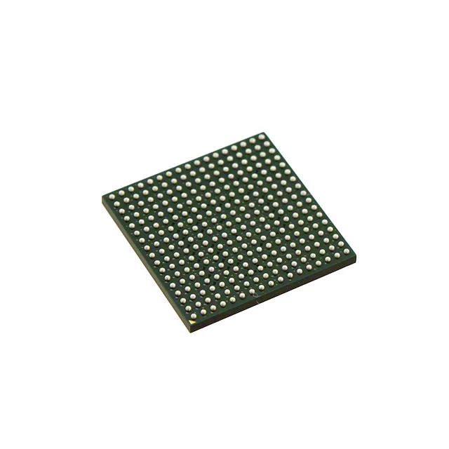
NXP Semiconductors MCIMX287CVM4B — Analog & Data Acquisition

NXP MCIMX287CVM4B i.MX28 MPU, ARM926EJ-S 454MHz

MPNMCIMX287CVM4B
End of Life

NXP i.MX28 series applications processor, MCIMX287CVM4B, ARM926EJ-S core at 454MHz, 289-MAPBGA, -40 to 85°C, dual USB 2.0 + PHY, 10/100 Ethernet, LVDDR/LVDDR2/DDR2 memory interface.

$27.08Ref. price · indicative, final on quote
Packaging289-LFBGA
StockContact for availability
MOQ1 pcs
  • 100% new & originalTraceable channels only — no refurbs, no pulls, no remarked parts.
  • Date & lot codes on quoteStated per line before you commit; label photos on request.
  • MSL-compliant ESD packingMoisture-sealed bags with indicator cards; reels photo-verified.
  • PayPal buyer protectionPay by T/T, PayPal or Payoneer — card payments covered end to end.

Specifications

MCIMX287CVM4B Technical Specifications
ParameterValue
Seriesi.MX28
Mounting typeSurface Mount
Voltage - i (O)1.8V, 3.3V
Additional interfacesCAN, I²C, I²S, MMC/SD/SDIO, SAI, SPI, SSI, SSP, UART
Display & interface controllersKeypad, LCD, Touchscreen
Operating temperature-40°C ~ 85°C (TA)
Number of cores (Bus width)1 Core, 32-Bit
USBUSB 2.0 + PHY (2)
Speed454MHz
PackageTray
Ethernet10/100Mbps (1)
Core processorARM926EJ-S
Case289-LFBGA
RAM controllersLVDDR, LVDDR2, DDR2
Co-Processors (DSP)Data; DCP
Security featuresBoot Security, Cryptography, Hardware ID
Graphics accelerationNo

Product details

ARM926EJ-S at 454 MHz — what it means for your system

The NXP MCIMX287CVM4B is an i.MX28 series applications processor built around a single ARM926EJ-S core running at 454 MHz. This is a 32-bit RISC core with a 5-stage pipeline, MMU for full OS support (Linux, RTOS), and DSP instruction extensions for basic signal processing. It is not a Cortex-A class part — expect it to handle HMI, protocol bridging, and data logging, not heavy multimedia or high-frame-rate graphics. The 454 MHz clock is the practical ceiling for sustained integer workloads in this process node. For a control-loop or protocol-stack application, you will typically run it below that to balance power. The part includes a DCP (Data Co-Processor) for cryptographic offload — AES, SHA, RSA — which keeps the ARM core free for application code when encrypting data streams or validating firmware signatures.

Industrial temperature range — field-ready from the start

Rated for -40°C to 85°C ambient, this part is specced for factory-floor controllers, outdoor telecom base stations, and any enclosure that sees seasonal temperature swings. No commercial-grade derating needed — the silicon and package are qualified for the full industrial band. If your system lives in a conditioned server room, you are paying for margin you do not need, but for anything with a fan or a roof, this is the right grade.

Integrated connectivity — USB and Ethernet on-chip

Two USB 2.0 ports with integrated PHY and a single 10/100 Mbps Ethernet MAC are built into the die. That means no external PHY for the USB (saves a chip and a crystal), and one Ethernet PHY chip on the BOM instead of a separate MAC+PHY combo. For a dual-USB host or OTG design, the on-chip PHY keeps the routing tight and the USB signal integrity predictable. The Ethernet MAC supports MII/RMII, so you can pick a PHY that matches your board's layer count.

Memory interface — LVDDR, LVDDR2, DDR2

The memory controller supports LVDDR, LVDDR2, and DDR2 SDRAM. That is a wider range than many MPUs of this generation — you are not locked into a single memory type. For cost-sensitive designs, LVDDR (1.8 V) keeps the PCB simpler; for higher bandwidth, DDR2 gives you faster data rates. The 289-MAPBGA package routes the DDR signals cleanly on a 4-layer board if you follow the layout guidelines for trace length matching.

Package and footprint — 289-MAPBGA, 14x14 mm

Housed in a 289-ball MAPBGA measuring 14x14 mm with a 0.8 mm ball pitch. That pitch is manageable with standard PCB fab — no micro-vias or HDI required, though a 4-layer board with via-in-pad might need filled vias. The package is RoHS3 compliant and MSL 3 out of the bag, so bake before reflow if the moisture barrier bag has been open longer than the floor-life window.

Security features — boot security and cryptography on-chip

Includes boot security (secure boot from NAND or SD), cryptography acceleration via the DCP, and a hardware unique ID. For a product that needs firmware anti-cloning or encrypted OTA updates, these blocks save you an external secure element. The hardware ID can be used for node authentication in an IoT or edge-compute network.

Lifecycle and sourcing — active, no end-of-life pressure

The MCIMX287CVM4B carries an active lifecycle status from NXP.

Frequently asked questions

What is the core processor and speed of NXP MCIMX287CVM4B?

The core is an ARM926EJ-S, a 32-bit RISC processor, running at 454 MHz. It includes an MMU for full OS support and DSP instruction extensions.

Can MCIMX287CVM4B be used for industrial applications?

Yes. It is rated for -40°C to 85°C ambient, which covers factory-floor, outdoor telecom, and other industrial environments. The integrated USB and Ethernet also suit it for industrial HMI and protocol gateway designs.

What are the differences between MCIMX287CVM4B and MCIMX283CVM4B?

The MCIMX287CVM4B runs at 454 MHz and includes a DCP co-processor for cryptographic acceleration, plus security features like boot security and hardware ID. The MCIMX283CVM4B is a lower-cost variant without the DCP and security block, typically running at a lower clock speed. Both share the same ARM926EJ-S core and 289-MAPBGA package, so they are pin-compatible for a drop-in upgrade if the design needs encryption offload.