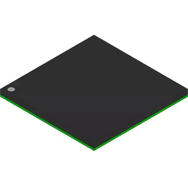
NXP Semiconductors MCF53014CMJ240 — Discrete Semiconductors

MCF53014CMJ240 ColdFire V3 MCU, 240 MHz, ROMless, 256-MAPBGA

MPNMCF53014CMJ240
End of Life

NXP MCF5301x MCF53014CMJ240 32-Bit ColdFire V3 MCU, 240 MHz, ROMless, 128K x 8 RAM, 83 I/O, Ethernet, USB OTG, 256-MAPBGA, -40 to 85°C.

$15.81Ref. price · indicative, final on quote
Packaging256-LBGA
StockContact for availability
MOQ1 pcs
  • 100% new & originalTraceable channels only — no refurbs, no pulls, no remarked parts.
  • Date & lot codes on quoteStated per line before you commit; label photos on request.
  • MSL-compliant ESD packingMoisture-sealed bags with indicator cards; reels photo-verified.
  • PayPal buyer protectionPay by T/T, PayPal or Payoneer — card payments covered end to end.

Specifications

MCF53014CMJ240 Technical Specifications
ParameterValue
SeriesMCF5301x
Mounting typeSurface Mount
Oscillator typeInternal
Program memory typeROMless
Voltage - supply (Vcc (Vdd))1.08V ~ 3.6V
Operating temperature-40°C ~ 85°C (TA)
Speed240MHz
PackageBulk
RAM size128K x 8
Core size32-Bit Single-Core
PeripheralsDMA, PWM, WDT
ConnectivityEBI/EMI, Ethernet, I²C, Memory Card, SPI, SSI, UART/USART, USB, USB OTG
Number of i (O)83
Core processorColdfire V3
Case256-LBGA

Product details

What this ColdFire V3 brings to a control board

The NXP MCF53014CMJ240 is a 32-bit ColdFire V3 microcontroller clocked at 240 MHz, built for applications that need a real-time control core with integrated networking. It runs from external program memory — the device is ROMless, so your BOM carries a separate Flash or boot ROM on the EBI/EMI bus. On-chip RAM is 128K x 8, enough for packet buffers and stack without external SRAM in many designs. The peripheral set includes DMA, PWM, and a watchdog timer, plus a rich connectivity block: Ethernet MAC, USB OTG, I²C, SPI, SSI, UART/USART, and a memory card interface. That mix makes it a fit for industrial Ethernet nodes, protocol converters, and embedded gateway boards where the CPU handles both control loops and network stacks.

240 MHz — what it buys on the bus

The 240 MHz core speed puts this part in a performance tier above the typical 72 MHz Kinetis K-series MCU (e.g. MK51DX128CMC7). That clock advantage matters when the CPU is handling both a TCP/IP stack and a PWM loop at the same time. The ColdFire V3 architecture is a variable-length RISC design with a hardware multiplier and divide, so the 240 MHz figure translates to a real throughput gain on control math and protocol parsing, not just a higher frequency number.

Package and assembly

The 256-MAPBGA (17x17 mm) is a fine-pitch BGA. Plan on a stencil and reflow profile matched to the ROHS3-compliant solder balls.

Temperature range and environment

Rated for -40 to 85 °C ambient, this MCU is specified for industrial enclosures.

Lifecycle and sourcing

The MCF53014CMJ240 carries an Active lifecycle status from NXP — no end-of-life notice, no last-time-buy window. It is ROHS3 compliant. There is no official NXP replacement listed, and the MK51DX128CMC7 is a lower-performance Kinetis part, not a pin-compatible second source.

Frequently asked questions

Does MCF53014CMJ240 have internal Flash memory?

No, the MCF53014CMJ240 is ROMless — it has zero internal program memory. The design must boot from external Flash or ROM on the EBI/EMI bus.

Is MCF53014CMJ240 RoHS compliant?

Yes, it is ROHS3 compliant.