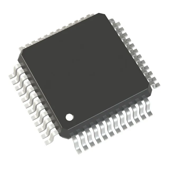
NXP Semiconductors MC56F82746VLFR — Analog & Data Acquisition

NXP MC56F82746VLFR 32-bit MCU, 100 MHz, 64 KB Flash, 48-LQFP

MPNMC56F82746VLFR
End of Life

NXP 56F8xxx series, MC56F82746VLFR, 32-Bit Single-Core MCU, 56800EX core, 100MHz, 64KB (32K x 16) FLASH, 4K x 16 RAM, 48-LQFP, -40°C to 105°C, 2.7V to 3.6V, CANbus, I2C, SCI, SPI, DMA, POR, PWM, WDT.

$10.57Ref. price · indicative, final on quote
Packaging48-LQFP
StockContact for availability
MOQ1 pcs
  • 100% new & originalTraceable channels only — no refurbs, no pulls, no remarked parts.
  • Date & lot codes on quoteStated per line before you commit; label photos on request.
  • MSL-compliant ESD packingMoisture-sealed bags with indicator cards; reels photo-verified.
  • PayPal buyer protectionPay by T/T, PayPal or Payoneer — card payments covered end to end.

Specifications

MC56F82746VLFR Technical Specifications
ParameterValue
Series56F8xxx
Mounting typeSurface Mount
Oscillator typeInternal
Program memory typeFLASH
Voltage - supply (Vcc (Vdd))2.7V ~ 3.6V
Operating temperature-40°C ~ 105°C (TA)
Speed100MHz
PackageTape & Reel (TR); Cut Tape (CT)
RAM size4K x 16
Core size32-Bit Single-Core
PeripheralsDMA, POR, PWM, WDT
ConnectivityCANbus, I2C, SCI, SPI
Number of i (O)39
Core processor56800EX
Case48-LQFP
Data convertersA/D 10x12b; D/A 2x12b
Program memory size64KB (32K x 16)

Product details

56800EX at 100 MHz — what it means for the control loop

The NXP MC56F82746VLFR is a 32-bit single-core MCU built around the 56800EX core, clocked at 100 MHz. It carries 64 KB of program Flash and 4K x 16 of RAM, enough for a moderate field-oriented control (FOC) stack or a CANopen node with local I/O. The 100 MHz rating is the real throughput ceiling for the DSP-style multiply-accumulate operations this core is designed for — expect a single-cycle MAC at that clock, which directly sets the PWM update rate and current-loop bandwidth in a motor-drive application.

Peripheral set for industrial connectivity

On the connectivity side you get CANbus, I2C, SCI (UART), and SPI — the usual set for linking to an inverter stage, an encoder interface, or a fieldbus gateway. The 39 I/O lines in the 48-LQFP package leave room for a few local sensors and a keypad or display. The integrated PWM and DMA peripherals offload the core for time-critical tasks like dead-time insertion and ADC synchronization.

Package and footprint

The 48-LQFP (7x7 mm) body is a common footprint shared across the 56F8xxx family. The exposed pad (if present — check the mechanical drawing) should be stitched to ground with thermal vias if the part dissipates more than a few hundred milliwatts.

Lifecycle and sourcing posture

The MC56F82746VLFR is listed as Active with ROHS3 compliance.

Frequently asked questions

Is there an equivalent or replacement for MC56F82746VLFR?

The 56F8xxx family includes pin-compatible variants with different Flash and RAM sizes. For a drop-in replacement with the same 48-LQFP footprint, compare the MC56F82746VLC (non-reel) or higher-density siblings like the MC56F83683VLFR. Verify the exact memory and peripheral match against the application requirements.

How to program MC56F82746VLFR?

Programming uses the standard 56800E toolchain — NXP's CodeWarrior for MCU or a third-party IDE with JTAG/SWD support. The internal oscillator eliminates the need for an external clock source, simplifying the programming interface to just power, ground, and a debug probe.

Is MC56F82746VLFR lead-free?

Yes, it is ROHS3 compliant, meaning it meets the latest EU restriction on hazardous substances including lead.