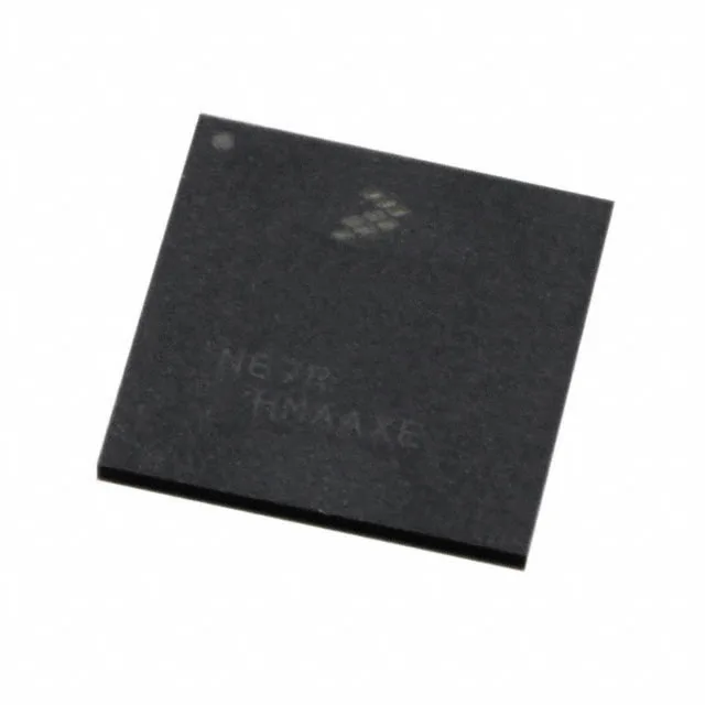
NXP Semiconductors LS1012ASE7EKA — DC-DC Power Modules

NXP LS1012ASE7EKA QorIQ Layerscape MPU, 600 MHz, 211-FCLGA

MPNLS1012ASE7EKA
End of Life

NXP QorIQ® Layerscape LS1012ASE7EKA, single-core ARM® Cortex®-A53 64-bit MPU at 600 MHz, USB 2.0 (1) + USB 3.0 with PHY, SATA 6Gbps (1), dual GbE, DDR3L, Secure Boot and TrustZone, 211-FCLGA (9.6x9.6 mm), 0 to 105 °C, tray.

$35.13Ref. price · indicative, final on quote
Packaging211-VFLGA
StockContact for availability
MOQ1 pcs
  • 100% new & originalTraceable channels only — no refurbs, no pulls, no remarked parts.
  • Date & lot codes on quoteStated per line before you commit; label photos on request.
  • MSL-compliant ESD packingMoisture-sealed bags with indicator cards; reels photo-verified.
  • PayPal buyer protectionPay by T/T, PayPal or Payoneer — card payments covered end to end.

Specifications

LS1012ASE7EKA Technical Specifications
ParameterValue
SeriesQorIQ® Layerscape
Mounting typeSurface Mount
Operating temperature0°C ~ 105°C
Number of cores (Bus width)1 Core, 64-Bit
USBUSB 2.0 (1), USB 3.0 + PHY
SATASATA 6Gbps (1)
Speed600MHz
PackageTray
EthernetGbE (2)
Core processorARM® Cortex®-A53
Case211-VFLGA
RAM controllersDDR3L
Security featuresSecure Boot, TrustZone®

Product details

I/O complement: USB 3.0, SATA 6Gbps, dual GbE

This MPU carries one USB 3.0 port with integrated PHY, one SATA 6 Gbps port, and two Gigabit Ethernet MACs. The USB 3.0 + PHY saves an external transceiver; the SATA port connects directly to a storage drive or SSD. The dual GbE ports support bridging or a WAN/LAN split in a gateway design. One USB 2.0 port is also present for lower-speed peripherals.

Memory interface: DDR3L only

The RAM controller is specified for DDR3L only — no DDR4 or LPDDR4 support. If your BOM calls for DDR3L, this part fits; if the design targets DDR4, this is the wrong memory interface. The single-channel DDR3L controller is adequate for the single-core's bandwidth needs in the target applications.

Package and assembly: 211-FCLGA, 9.6x9.6 mm

The LS1012ASE7EKA comes in a 211-ball FCLGA package, 9.6 mm square. It is a surface-mount LGA — no balls to reflow, just a land-grid array. The tray shipping medium is what you get; this variant is not offered in tape and reel. The small footprint suits space-constrained designs, but the LGA package requires a solder-paste stencil and reflow profile tuned for leadless packages.

Temperature grade: 0 to 105 °C

Rated for 0 °C to 105 °C operating junction temperature.

Security features: Secure Boot and TrustZone

Hardware security includes Secure Boot and ARM TrustZone. Secure Boot verifies the bootloader signature before execution; TrustZone creates a trusted execution environment for cryptographic keys and secure firmware updates. These are standard for IoT edge nodes and gateway products that need to resist firmware tampering.

Lifecycle and sourcing

No end-of-life notice or last-time-buy window is in effect. This is a current, catalogued part available through the independent distribution channel.

Frequently asked questions

Is LS1012ASE7EKA compatible with DDR3L?

Yes, the RAM controller is specified for DDR3L. DDR4 and LPDDR4 are not supported on this part.

Does LS1012ASE7EKA have secure boot and TrustZone?

Yes, it includes Secure Boot and ARM TrustZone hardware security features for verified boot and trusted execution.

What is the difference between LS1012ASE7EKA and LS1012AXE7EKA?

The LS1012AXE7EKA is a different speed-grade or feature-set variant within the same LS1012 family. The 'SE7' suffix on this part indicates the 600 MHz speed grade. Pin compatibility across the LS1012 family should be verified against the NXP datasheet for the specific package and feature set.