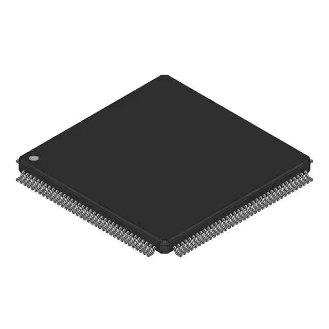
NXP LPC18S10FBD144551 ARM Cortex-M3 MCU, 180MHz, 83 I/O, 144-LQFP
NXP LPC18S10FBD144551, LPC18xx series, 32-bit ARM Cortex-M3 single-core at 180MHz, ROMless external-flash architecture, 2.2–3.6 V supply, 144-LQFP (20×20mm), 83 I/O, CANbus, 8×10b ADC, 1×10b DAC, DMA, SD/MMC, -40°C to 85°C, Active.
- 100% new & originalTraceable channels only — no refurbs, no pulls, no remarked parts.
- Date & lot codes on quoteStated per line before you commit; label photos on request.
- MSL-compliant ESD packingMoisture-sealed bags with indicator cards; reels photo-verified.
- PayPal buyer protectionPay by T/T, PayPal or Payoneer — card payments covered end to end.
Specifications
| Parameter | Value |
|---|---|
| Series | LPC18xx |
| Mounting type | Surface Mount |
| Oscillator type | Internal |
| Program memory type | ROMless |
| Voltage - supply (Vcc (Vdd)) | 2.2V ~ 3.6V |
| Operating temperature | -40°C~85°C(TA) |
| Speed | 180MHz |
| Package | Bulk |
| RAM size | 136K x 8 |
| Core size | 32-Bit Single-Core |
| Peripherals | Brown-out Detect/Reset, DMA, I²S, POR, PWM, WDT |
| Connectivity | CANbus, EBI/EMI, I²C, IrDA, Microwire, MMC/SD, SPI, SSI, SSP, UART/USART |
| Number of i (O) | 83 |
| Core processor | ARM® Cortex®-M3 |
| Case | 144-LQFP |
| Data converters | A/D 8x10b; D/A 1x10b |
Frequently asked questions
What does ROMless mean for ordering and firmware development on the LPC18S10FBD144551?
ROMless means the part has no internal flash — program code lives on an external memory device connected via the EBI/EMI parallel bus interface. A boot-loader must be resident on the external flash before first power-up, and the firmware build must target the external memory map. For procurement this adds an external flash device to the BOM as a hard dependency. For commissioning it means the startup sequence involves both the MCU and the external flash device — a two-part bring-up instead of a single-chip load.
Does the 144-LQFP (20×20mm) footprint of the LPC18S10 match existing 144-pin ARM layouts, and is it a direct swap for flash-backed LPC18xx variants?
The 144-pin count and LQFP package are consistent with the NXP LPC18xx footprint standard, but the ROMless design changes the BOM composition: a flash-backed variant (LPC18x7 series) carries the program memory on-die and needs no external flash bus. The LPC18S10 requires the EBI/EMI interface to be routed and populated, so it is not a mechanical-only drop-in swap — the board must support the parallel bus to the external memory device. Layout compatibility is confirmed by verifying the EBI bus routing exists on the target board, not just that the pin pitch and package outline match.
Is the 136K on-chip RAM sufficient for a full RTOS stack with dual CANopen and SD card logging?
The 136K of on-chip SRAM is the available RAM budget for all firmware purposes — kernel heap, task stacks, CANopen session buffers, SD card DMA buffers, and application variables share that pool. Dual CANopen stacks at full PDO count plus SD card write buffers can consume 80–100K of that budget depending on configuration and message queue depth, leaving a constrained working margin at 136K. A firmware footprint analysis against the specific uC/OS-III build and SD card library in use is required before the BOM line is frozen — the RAM ceiling is real and not inferred from any datasheet note, bu