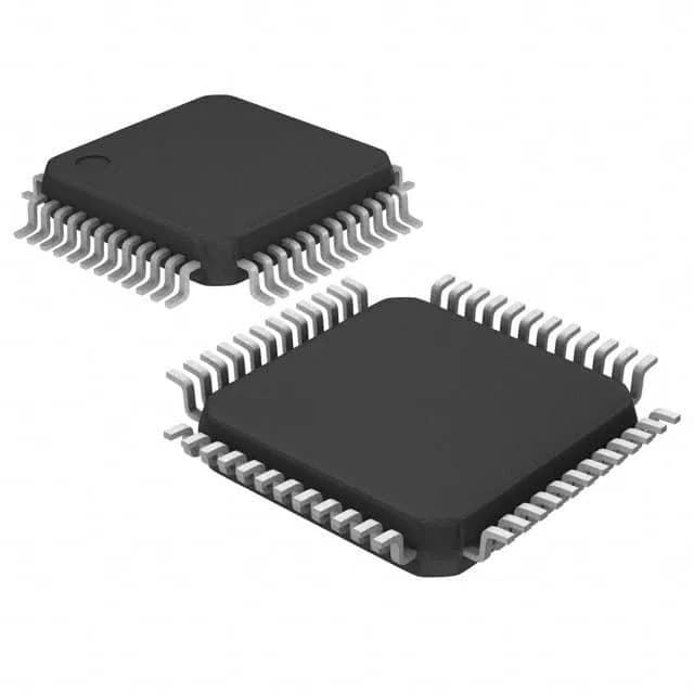
NXP LPC11U68JBD48K MCU, ARM Cortex-M0+ 50MHz, 256KB Flash, USB, 48-LQFP
NXP LPC11Uxx series, 32-bit ARM Cortex-M0+ at 50MHz, 256KB Flash, 36KB RAM, 4KB EEPROM, USB/I2C/SPI/SSP/UART, 8×12-bit SAR ADC, 34 I/O, -40°C to 105°C, 2.4–3.6V, 48-LQFP (7×7mm) Tray.
- 100% new & originalTraceable channels only — no refurbs, no pulls, no remarked parts.
- Date & lot codes on quoteStated per line before you commit; label photos on request.
- MSL-compliant ESD packingMoisture-sealed bags with indicator cards; reels photo-verified.
- PayPal buyer protectionPay by T/T, PayPal or Payoneer — card payments covered end to end.
Specifications
| Parameter | Value |
|---|---|
| Series | LPC11Uxx |
| Mounting type | Surface Mount |
| Oscillator type | Internal |
| Program memory type | FLASH |
| Voltage - supply (Vcc (Vdd)) | 2.4V ~ 3.6V |
| Operating temperature | -40°C~105°C(TA) |
| Speed | 50MHz |
| Package | Tray |
| RAM size | 36K x 8 |
| Core size | 32-Bit Single-Core |
| EEPROM size | 4K x 8 |
| Peripherals | Brown-out Detect/Reset, DMA, POR, PWM, WDT |
| Connectivity | I²C, Microwire, SmartCard, SPI, SSP, UART/USART, USB |
| Number of i (O) | 34 |
| Core processor | ARM® Cortex®-M0+ |
| Case | 48-LQFP |
| Data converters | A/D 8x12b SAR |
| Program memory size | 256KB (256K x 8) |
Frequently asked questions
Does the LPC11U68JBD48K support SWD debug and which ARM toolchains are validated for LPC11Uxx?
The LPC11Uxx series supports SWD debug via the ARM CoreSight debug interface — Keil MDK, IAR Embedded Workbench, and GCC (via OpenOCD or J-Link) are the three toolchains NXP validates for this family. Confirm the LPC11U68JBD48K-specific device pack is loaded in your IDE before flashing.
What is the minimum VDD operating range — does it sit comfortably on a 3.3V ±5% industrial rail?
The minimum supply is 2.4V. A 3.3V ±5% rail (3.135–3.465V) sits well inside the 2.4–3.6V operating window — no level-shifting needed. Watch brown-out: the rail must not sag below 2.4V during USB transmit bursts or motorised IO switching events; the on-chip BOD peripheral should be configured to catch those dips before firmware runs off the rails.
How does the LPC11U68JBD48K compare to the LPC11U37JBD48K on ADC and I/O?
Both carry the same 8×12-bit SAR ADC and the same 48-LQFP pin count — the I/O budget is 34 on both. The memory delta is the selection driver: the LPC11U68JBD48K doubles the Flash to 256KB and bumps RAM to 36KB versus the LPC11U37JBD48K's lower tiers. If the existing layout is locked, the ADC and I/O count are a straight carry-over; recompile is required for the memory change.