80 MHz 56800 core — what the speed buys in a control loop
The NXP DSP56F805FV80E is a 16-bit MCU built around the 56800 core, clocked at 80 MHz. That clock rate is the headline spec that decides whether your motor-drive or power-conversion loop closes fast enough.
64 KB Flash and 2K x 16 RAM — sizing the firmware budget
Program memory is 64 KB of Flash (32K x 16), and data RAM is 2K x 16. For a dedicated motor-control or industrial-control application, 64 KB is enough for a modest control stack plus bootloader and calibration tables. The 2K x 16 RAM is tight for a large lookup table or a double-buffered commutation schedule — you will want to allocate critical variables to the on-chip RAM and stream the rest from Flash. If your algorithm needs more working memory, the EBI/EMI interface on this part lets you hang external SRAM or a serial memory off the bus.
On-chip peripherals — what stays off the BOM
The peripheral set includes a POR (power-on reset), a PWM module, a watchdog timer, a CAN 2.0B controller, a SCI (UART), and an SPI port. That means you can skip an external supervisor IC (POR and WDT cover that), an external CAN transceiver interface (the CAN controller is on-chip — just add a transceiver), and a separate ADC. The 8-channel 12-bit ADC samples at rates adequate for current sensing in a motor drive or voltage monitoring in a power supply. For a typical three-phase motor controller, the PWM module and ADC together handle the timing and feedback without external glue logic.
Package and temperature grade — field-swap reality
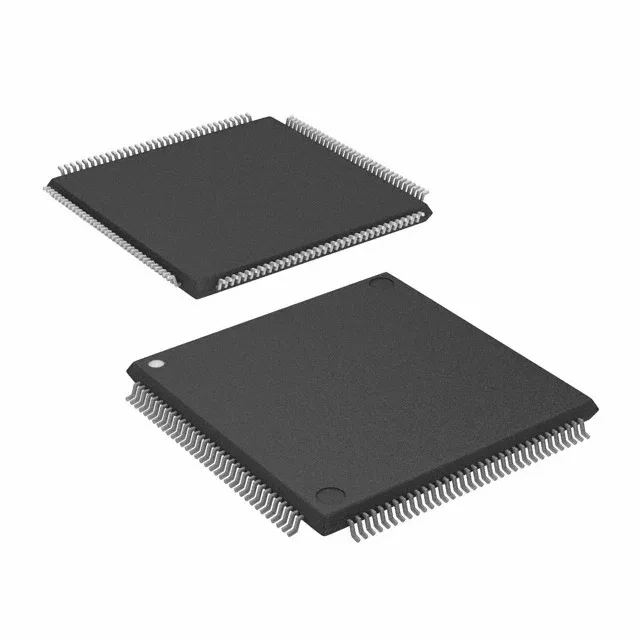
The part comes in a 144-pin LQFP (20x20 mm body). That is a fine-pitch QFP — reworkable with a hot-air station and a stencil if you are on site, but not something you swap with a soldering iron alone.
NXP lists the DSP56F805FV80E as Active, and it is ROHS3 compliant.