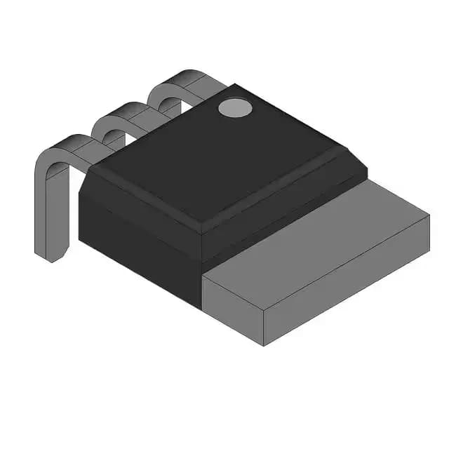
With a maximum Rds(on) of 3.1 mOhm at 25 A gate-driven to 10 V, it targets high-efficiency switching in automotive power distribution, DC-DC converters, motor pre-drive stages, and reverse-battery protection circuits. The through-hole I2PAK package handles the 234 W power dissipation budget required in engine bay and chassis-domain environments.
This part carries an Automotive grade designation and is AEC-Q101 qualified, which means it meets the stress test and reliability requirements for automotive applications including under-hood and transmission-attached modules. The qualification documentation supports PPAP submission for Tier-1 and OEM programs.
3.1 mOhm Rds(on) — the switching loss trade-off
The maximum on-resistance of 3.1 mOhm at 10 V gate drive is among the lowest for a 40 V through-hole MOSFET in this package class. The 79 nC typical gate charge at 10 V means the driver must deliver a 79 nC pulse per switching cycle; pair this with a gate driver rated for at least 2 A peak to keep transition times under 50 ns at 100 A. The 6200 pF input capacitance at 25 V drain-source adds to the drive demand — budget gate-drive power accordingly.
Package and mounting
The I2PAK (TO-262) through-hole package suits designs where a heatsink is mounted directly to the device tab, common in automotive power modules. The through-hole leads handle the 100 A continuous drain current when the tab is properly heat-sunk to the PCB or chassis.