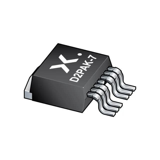
NXP Semiconductors BUK6C3R3-75C,118 — Logic ICs

Nexperia BUK6C3R3-75C,118 N-Channel MOSFET, 75 V, 3.4 mOhm

MPNBUK6C3R3-75C,118
End of Life

Nexperia TrenchMOS™ BUK6C3R3-75C,118, N-Channel MOSFET, 75 V Vdss, 181 A Id, 3.4 mOhm Rds(on) at 10 V, D2PAK-7, AEC-Q101, -55 to 175 °C.

$1.47Ref. price · indicative, final on quote
PackagingD2PAK-7
StockContact for availability
MOQ1 pcs
  • 100% new & originalTraceable channels only — no refurbs, no pulls, no remarked parts.
  • Date & lot codes on quoteStated per line before you commit; label photos on request.
  • MSL-compliant ESD packingMoisture-sealed bags with indicator cards; reels photo-verified.
  • PayPal buyer protectionPay by T/T, PayPal or Payoneer — card payments covered end to end.

Specifications

BUK6C3R3-75C,118 Technical Specifications
ParameterValue
SeriesTrenchMOS™
FET typeN-Channel
Mounting typeSurface Mount
Drain to source voltage75 V
Drive voltage (Max rds on, min rds on)10V
Current - continuous drain (Id) @ 25°C181A (Tc)
Power dissipation300W (Tc)
Operating temperature-55°C ~ 175°C (TJ)
GradeAutomotive
PackageBulk
Vgs±16V
TechnologyMOSFET (Metal Oxide)
QualificationAEC-Q101
Vgs(th) (Max) @ id2.8V @ 1mA
Rds on (Max) @ id, vgs3.4mOhm @ 90A, 10V
Gate charge (Qg) (Max) @ vgs253 nC @ 10 V
Input capacitance (Ciss) (Max) @ vds15800 pF @ 25 V

Product details

What this N-channel TrenchMOS™ MOSFET does in the circuit

The D2PAK-7 surface-mount package handles the 300 W dissipation budget when the thermal pad is properly stitched to the board's copper plane.

At 90 A load current with 10 V gate drive, the 3.4 mOhm maximum on-resistance translates to roughly 28 W of conduction loss at the rated current. That is well within the 300 W power dissipation ceiling, but the real-world junction temperature depends on how effectively the D2PAK-7's exposed pad is soldered to a large copper area.

Automotive qualification and temperature range

The ±16 V maximum gate-to-source rating gives margin for noisy 12 V and 24 V electrical systems. Nexperia lists no direct successor, so the BUK6C3R3-75C,118 is the current-generation part for new designs.

Package and footprint considerations

Surface-mount D2PAK-7 (TO-263-7 variant) with the exposed drain pad on the backside. The 15800 pF input capacitance at 25 V drain bias means the gate driver sees a significant capacitive load — a gate resistor in the 1 Ω to 10 Ω range damps ringing without slowing the turn-on too much. The 2.8 V maximum gate threshold at 1 mA drain current confirms it is a logic-level device, but the 10 V drive voltage for minimum Rds(on) is the recommended operating point for full performance.

Frequently asked questions

Is BUK6C3R3-75C,118 AEC-Q101 qualified?

Yes, it carries AEC-Q101 qualification, making it suitable for automotive applications where the part must meet the stress and reliability requirements of the AEC-Q101 standard.

What is the replacement for BUK6C3R3-75C,118?

No official successor is listed. The BUK6C3R3-75C,118 itself is the active part; for a second-source candidate, look for an AEC-Q101 N-channel MOSFET in D2PAK-7 with similar 75 V, 3.4 mOhm ratings, but confirm pin compatibility and gate drive requirements against your design.

What are the specifications of BUK6C3R3-75C,118?

Packaged in surface-mount D2PAK-7.