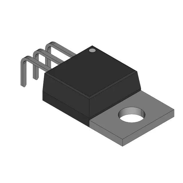
NXP Semiconductors BUJ303B,127 — Logic ICs

BUJ303B,127 NPN Power Transistor, 400 V, 5 A, TO-220

MPNBUJ303B,127
End of Life

WeEn Semiconductor BUJ303B,127 NPN power bipolar transistor, 400 V Vce, 5 A Ic, 100 W, TO-220AB through-hole, 150°C junction temperature.

$0.36Ref. price · indicative, final on quote
PackagingTO-220-3
StockContact for availability
MOQ1 pcs
  • 100% new & originalTraceable channels only — no refurbs, no pulls, no remarked parts.
  • Date & lot codes on quoteStated per line before you commit; label photos on request.
  • MSL-compliant ESD packingMoisture-sealed bags with indicator cards; reels photo-verified.
  • PayPal buyer protectionPay by T/T, PayPal or Payoneer — card payments covered end to end.

Specifications

BUJ303B,127 Technical Specifications
ParameterValue
Mounting typeThrough Hole
FET typeNPN
Voltage - collector emitter breakdown400 V
Current - collector (Ic)5 A
Current - collector cutoff100µA
DC current gain (hFE) (Min) @ ic, vce23 @ 800mA, 3V
Power - max100 W
Operating temperature150°C (TJ)
PackageBulk
CaseTO-220-3
Vce saturation (Max) @ ib, ic1.5V @ 1A, 3A

Product details

400 V Vce, 5 A Ic — the switching transistor for mains-referenced circuits

The BUJ303B,127 from WeEn Semiconductor is an NPN power bipolar transistor in a TO-220AB through-hole package. Its 400 V collector-emitter breakdown voltage and 5 A continuous collector current make it a fit for line-voltage switching applications — flyback clamps, electronic ballasts, switch-mode power supply primary-side drivers, and motor control snubbers where a 400 V blocking rating is the minimum for 240 VAC rectified rails.

100 W power dissipation — thermal budget for the design

Rated for 100 W maximum power dissipation, this part needs a heatsink for any continuous load above a few watts. The TO-220AB metal tab is the primary thermal path — plan for a thermal pad or mica insulator and a properly sized heatsink. The junction temperature limit is 150°C, so derate the power based on the thermal resistance of your mounting arrangement.

The Vce(sat) is 1.5 V maximum at 1 A base current and 3 A collector current. That 1.5 V drop at 3 A means 4.5 W conduction loss in the transistor alone — a figure that directly factors into the heatsink sizing and the overall efficiency budget. The DC current gain (hFE) is a minimum of 23 at 800 mA collector current and 3 V Vce. This moderate gain means the base drive circuit must supply roughly 35 mA to saturate the transistor at 800 mA load; at the full 5 A rating the required base current will be higher, so the driver stage needs to be sized accordingly.

Frequently asked questions

Is BUJ303B suitable for 400 V applications?

Yes. The collector-emitter breakdown voltage is rated at 400 V maximum, which means the transistor can block 400 V in the off state. This makes it suitable for circuits operating on rectified 240 VAC mains (typical peak ~340 V) or other 400 V bus applications, provided the switching and conduction losses stay within the 100 W power dissipation limit.

What is the hFE of BUJ303B?

This is a moderate gain figure typical of a power transistor — the base drive circuit must supply adequate current to saturate the device at the intended load.