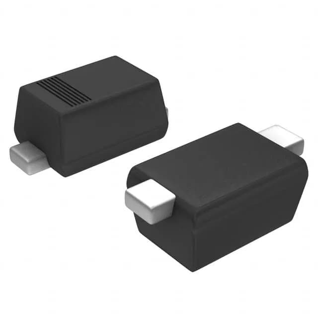
NXP Semiconductors BAP64-02,115

NXP BAP64-02,115 PIN Diode, 0.35pF at 20V, SOD-523

MPNBAP64-02,115
End of Life

NXP BAP64-02,115 single PIN diode, 175V peak reverse, 100 mA max, 1.35 ohm at 100mA/100MHz, 0.35 pF at 20V/1MHz, 715 mW, SOD-523, -65 to 150°C.

$0.39Ref. price · indicative, final on quote
PackagingSC-79, SOD-523
StockContact for availability
MOQ1 pcs
  • 100% new & originalTraceable channels only — no refurbs, no pulls, no remarked parts.
  • Date & lot codes on quoteStated per line before you commit; label photos on request.
  • MSL-compliant ESD packingMoisture-sealed bags with indicator cards; reels photo-verified.
  • PayPal buyer protectionPay by T/T, PayPal or Payoneer — card payments covered end to end.

Specifications

BAP64-02,115 Technical Specifications
ParameterValue
Diode typePIN - Single
Voltage - peak reverse175V
Current - max100 mA
Power dissipation715 mW
Operating temperature-65°C ~ 150°C (TJ)
PackageTape & Reel (TR); Cut Tape (CT)
CaseSC-79, SOD-523
Resistance @ if, f1.35Ohm @ 100mA, 100MHz
Capacitance @ vr, f0.35pF @ 20V, 1MHz

Product details

0.35 pF at 20 V — off-state isolation in a SOD-523 footprint

The NXP BAP64-02,115 is a single PIN diode in the SOD-523 package, designed for RF switching and attenuator applications where low capacitance at reverse bias is the primary isolation lever. At 20 V reverse bias and 1 MHz, the capacitance measures 0.35 pF — low enough to keep the off-state port isolated well into the GHz range without adding a shunt inductor.

1.35 ohm series resistance — insertion loss in the on-state

Forward-biased at 100 mA and measured at 100 MHz, the series resistance is 1.35 ohm. This is the on-state insertion loss floor: lower resistance means less signal attenuation through the diode in the conducting state. The 100 mA maximum continuous current sets the bias ceiling for maintaining low Rds without exceeding the 715 mW power dissipation limit.

175 V peak reverse — high-voltage RF switching capability

The 175 V peak reverse voltage rating allows the part to handle RF signals with large voltage swings without forward-biasing into conduction.

The operating junction temperature range spans -65°C to 150°C, covering military avionics cold-soak and under-hood automotive hot-soak without derating. The 715 mW power dissipation limit assumes the SOD-523 solder pad is tied to a copper plane; in free-air the derating curve from the datasheet should be consulted for continuous bias above 85°C ambient.

Frequently asked questions

Is BAP64-02,115 suitable for RF switching?

Yes. The 0.35 pF capacitance at 20 V reverse bias and 1.35 ohm series resistance at 100 mA forward bias make it suited for RF switching and attenuator circuits up to several GHz. The 175 V peak reverse voltage also allows it to handle higher-power RF signals than typical 50 V or 100 V PIN diodes in the same package.

What is the capacitance of BAP64-02,115 at 20V?

The capacitance is 0.35 pF, measured at 20 V reverse bias and 1 MHz. This low value is the key parameter for maintaining off-state isolation in RF switch and attenuator designs.