RF PIN diode for switching and attenuator stages
The BAP55LX,315 is a single PIN diode from NXP, designed for RF switching, attenuator, and limiter circuits up to several GHz. Its key parametrics — 0.28 pF capacitance at 20 V and 800 mOhm series resistance at 100 mA — give the designer a clear trade-off between off-state isolation and on-state insertion loss.
Capacitance and resistance: the RF design trade-off
At 20 V reverse bias, the junction capacitance is 0.28 pF (measured at 1 MHz). That low value keeps the diode from coupling RF signal across the junction in the off state, which matters for isolation in T/R switches and shunt attenuators. Forward-biased at 100 mA (100 MHz), the series resistance drops to 800 mOhm. This on-state resistance directly sets the insertion loss through the diode; 800 mOhm is typical for a small-signal PIN diode in a 50-ohm system, adding roughly 0.07 dB loss per series element.
Package footprint and thermal reality
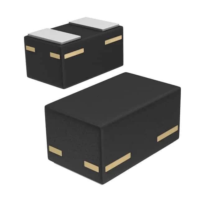
The diode comes in a 2-XDFN package (NXP designation DFN1006D-2), a 1.0 mm × 0.6 mm leadless package with two side-wettable terminations. Maximum power dissipation is 135 mW, so the thermal path relies on the PCB copper pad under the part — no exposed pad, so the solder fillet on the two terminals is the only heat sink.
Temperature range and voltage ceiling
Junction temperature range spans -65°C to 150°C, covering military and industrial environments. Peak reverse voltage is 50 V, which sets the RF voltage swing limit — for a 50-ohm system, that translates to roughly +34 dBm peak RF power before the diode self-biases into conduction.