AEC-Q100 quad NAND with Schmitt-trigger inputs — what the ratings mean for a 5V automotive logic rail
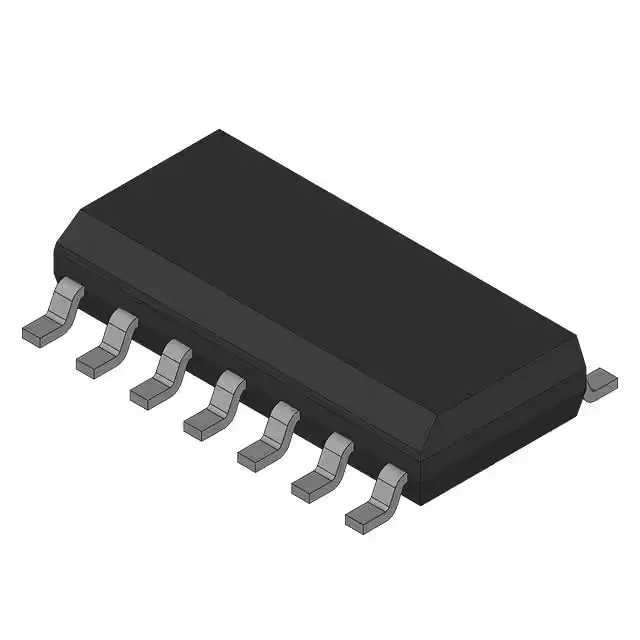
The 74HCT132D-Q100,118: Four independent 2-input NAND gates in a single 14-SOIC package, each with Schmitt-trigger input hysteresis. The Schmitt action cleans up slow edges from sensor outputs or long PCB traces before the gate toggles.
Switching speed and quiescent draw — the 33 ns propagation delay at 4.5V
Maximum propagation delay is 33 ns at 4.5V supply driving a 50 pF load. This sets the data-rate ceiling for a single gate: at 33 ns per transition, the practical toggle rate is about 15 MHz before the output edge degrades. For a 5V SPI bus running at 10 MHz, the gate's delay adds roughly one-third of a bit period — account for it in the setup-time budget if the gate is in the clock path. Quiescent current is 2 µA maximum. For a module that stays powered in key-off mode, four gates drawing 2 µA total adds negligible draw to the always-on 5V rail. The 4 mA symmetrical output drive (both high and low) is sized for driving CMOS logic inputs and short PCB traces up to about 30 pF — not for long backplane buses or 50-ohm terminated lines.
Active production — no end-of-life notice on record
The part ships in Bulk — tube or tray, not tape-and-reel. For high-volume pick-and-place, confirm the packaging option with your NXP source before committing the BOM line. The 14-SOIC footprint (3.90 mm body width) is standard across the 74HCT family, so a board layout already using 74HCT logic accepts this gate without a respin.