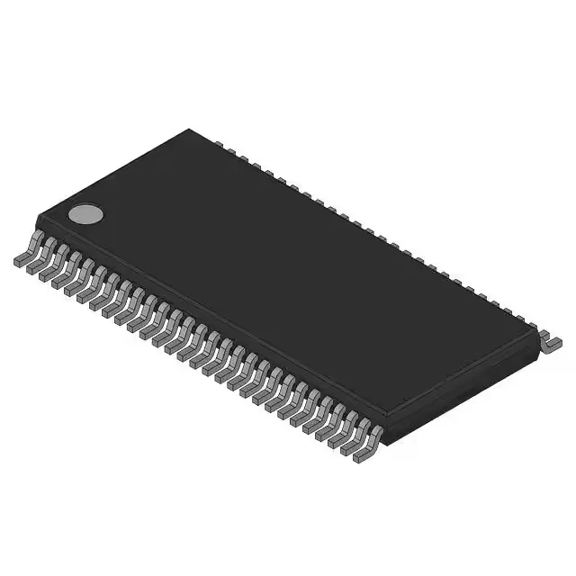
Dual 10-bit buffer for mixed-voltage bus translation
The NXP 74ALVT16827DGGS is a dual 10-bit non-inverting buffer with 3-state outputs, packaged in a 56-TSSOP. It accepts either a 2.3V–2.7V or a 3V–3.6V supply rail, making it a natural fit for boards that need to buffer a 2.5V bus on one side and a 3.3V bus on the other without an external level shifter. The 64 mA sink capability on each output is the headline drive figure — enough to handle heavily loaded backplane traces or large fan-out to multiple CMOS loads without signal degradation.
The supply is specified as two separate ranges — 2.3V to 2.7V and 3V to 3.6V — rather than a single continuous band. That means the part is designed for either a 2.5V nominal or a 3.3V nominal rail, not for a 2.8V or 3.0V midpoint. If your board runs a 2.8V supply, this buffer will not operate correctly; you need a part rated for that intermediate voltage. The 32 mA source / 64 mA sink asymmetry is deliberate: the stronger sink handles the capacitive discharge of long PCB traces or multiple gate inputs on the falling edge, which is where most signal-integrity margin is lost on a shared bus.
Package and mounting — 56-TSSOP footprint verification
The 56-TSSOP body (6.10 mm width) is a surface-mount package.
Lifecycle status — active, no LTB watch needed
The 74ALVT series remains a current logic family from NXP.