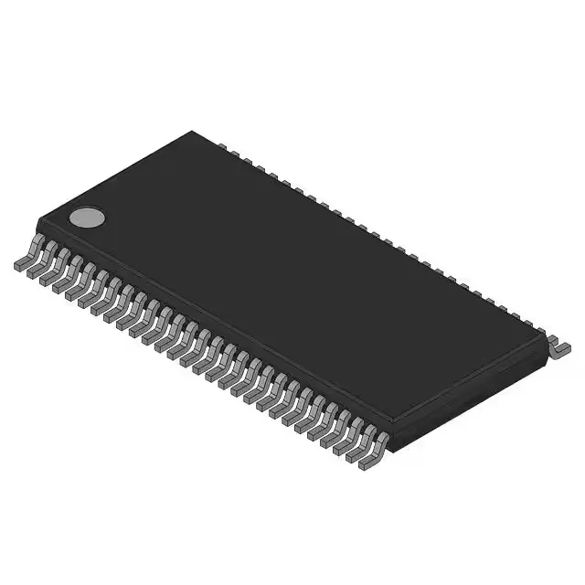
NXP Semiconductors 74ALVT16823DGG,118 — Microcontrollers & Processors (MCU / MPU / DSP)

74ALVT16823DGG,118 NXP 74ALVT D-Type Flip-Flop, 250 MHz

MPN74ALVT16823DGG,118
End of Life

NXP Semiconductors 74ALVT series D-Type flip-flop, 74ALVT16823DGG,118, dual 9-bit, positive edge trigger, tri-state non-inverted outputs, 250 MHz clock frequency, 56-TSSOP package.

$2.93Ref. price · indicative, final on quote
Packaging56-TFSOP (0.240", 6.10mm Width)
StockIn Stock (28)
Lead timeIn Stock wk
MOQ1 pcs
  • 100% new & originalTraceable channels only — no refurbs, no pulls, no remarked parts.
  • Date & lot codes on quoteStated per line before you commit; label photos on request.
  • MSL-compliant ESD packingMoisture-sealed bags with indicator cards; reels photo-verified.
  • PayPal buyer protectionPay by T/T, PayPal or Payoneer — card payments covered end to end.

Specifications

74ALVT16823DGG,118 Technical Specifications
ParameterValue
TypeD-Type
Series74ALVT
Output typeTri-State, Non-Inverted
Trigger typePositive Edge
Mounting typeSurface Mount
Voltage2.3V ~ 2.7V, 3V ~ 3.6V
Current - quiescent100 µA
Current - output high, low8mA, 24mA; 32mA, 64mA
Frequency250 MHz
Operating temperature-40°C ~ 85°C (TA)
PackageBulk
FunctionMaster Reset
Case56-TFSOP (0.240\", 6.10mm Width)
Input capacitance3 pF
Number of elements2
Number of bits per element9
Max propagation delay @ v, max CL3.1ns @ 3.3V, 50pF

Product details

Dual 9-bit D-type with 250 MHz clock ceiling

The 74ALVT16823DGG,118 is a dual 9-bit D-type flip-flop from NXP's 74ALVT series, with a master reset function and positive-edge triggering. Each element stores nine bits, giving 18 flip-flops in one 56-TSSOP package. Rated for a 250 MHz clock frequency, this part handles high-speed data pipelines where the upstream bus toggles at hundreds of megahertz. The 3.1 ns max propagation delay at 3.3 V, 50 pF load sets the timing budget for the downstream logic — a 250 MHz signal has a 4 ns period, so the 3.1 ns delay leaves roughly 0.9 ns of setup margin before the next clock edge.

Supply flexibility and output drive

The 100 µA quiescent current keeps the static power draw low in clock-gated designs. Outputs source 8 mA (high) and sink 24 mA (low) at the lower voltage range, and 32 mA source / 64 mA sink at 3.3 V. This drive strength is enough to fan out to multiple CMOS loads on a short PCB trace without external buffers.

Industrial temperature and package

The 56-TFSOP (6.10 mm width) and 56-TSSOP supplier package are both surface-mount — the 0.65 mm pitch requires a standard SMT assembly line with no special via-in-pad.