48 MHz Cortex-M0+ — what the speed buys you
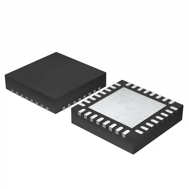
The NXP MKL05Z32VFM4 is a 32-bit ARM Cortex-M0+ MCU from the Kinetis KL0 series, built for ultra-low-power operation without giving up a 48 MHz core clock. That clock rate is enough for sensor fusion loops, basic motor commutation, or UART/I²C/SPI protocol handling in a power-constrained node. The 32 KB Flash and 4 KB RAM (4K x 8) set a firm firmware budget — fit for a single control loop with a modest bootloader, not a multi-stack RTOS. 28 I/O are available on the 32-HVQFN (5×5 mm) package, and the wettable flank option means AOI-visible solder joints, a practical advantage for high-yield assembly.
Rated for -40°C to 105°C (TA) and 1.71 V to 3.6 V supply range.
On-chip peripherals and integration
The part integrates a 14-channel 12-bit A/D converter and a single 12-bit D/A, enough for analog sensor inputs and a control output without external converters. Internal oscillator keeps the BOM count down; no external crystal needed for many applications.
ROHS3 compliant. For BOM-freeze planning, the base product number MKL05Z32 covers the Flash and RAM variants in the KL0 family, so a density upgrade within the same pinout is possible without a board spin.