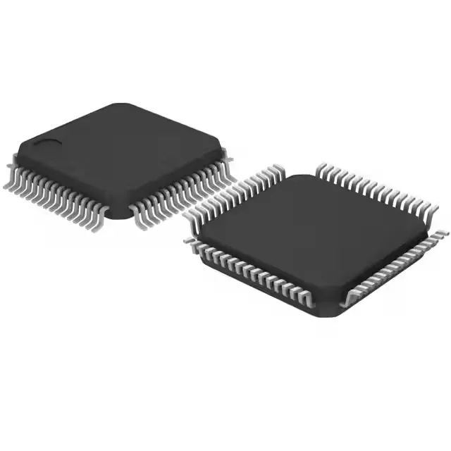
Dual-core at 100 MHz — what the asymmetric architecture buys you
The NXP LPC54113J256BD64QL is a 32-bit dual-core MCU pairing an ARM Cortex-M4 for DSP/FPU-heavy work with a Cortex-M0+ for control, comms, or housekeeping. The 100 MHz clock on both cores means the M4 can run a sensor-fusion or audio algorithm without the M0+ stalling on I²C or UART traffic. 256 KB flash and 192 KB RAM give enough room for a FreeRTOS-based application with a modest protocol stack, though a graphics frame buffer or large lookup table would push into external memory territory.
Peripherals and I/O — what is actually on the pins
The 12-channel 12-bit ADC is enough for reading a three-phase current-sense plus a thermistor and a potentiometer on a motor-drive board. DMA and I²S are present, so streaming audio or moving ADC samples to RAM without CPU intervention is supported.
Lifecycle and sourcing reality — active, no LTB pressure
ROHS3 compliant per the listing. The date-code and marking should trace cleanly to NXP's standard laser-etch font and package format — no reason to suspect gray-market re-marking on an active, widely-distributed part.