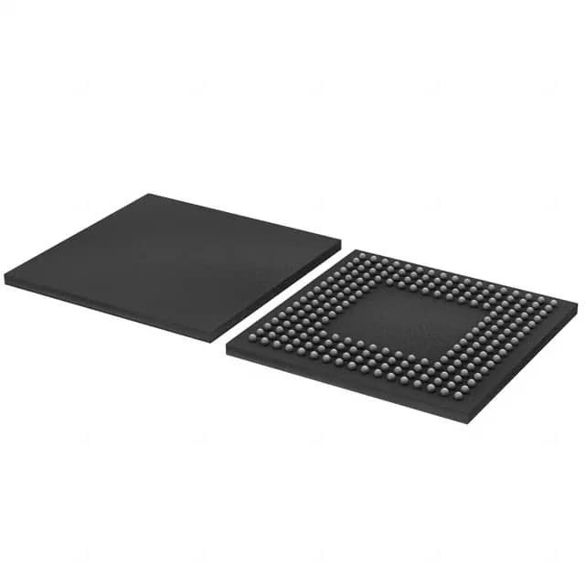
NXP LPC1788FET208,551 ARM Cortex-M3 MCU, 120MHz, 512KB Flash, 208-TFBGA
NXP LPC17xx series, 32-bit ARM Cortex-M3 at 120MHz, 512KB Flash, 96KB RAM, 165 I/O, Ethernet and USB OTG peripherals, 208-TFBGA surface-mount package, -40°C to 85°C operating temperature, ROHS3 compliant.
- 100% new & originalTraceable channels only — no refurbs, no pulls, no remarked parts.
- Date & lot codes on quoteStated per line before you commit; label photos on request.
- MSL-compliant ESD packingMoisture-sealed bags with indicator cards; reels photo-verified.
- PayPal buyer protectionPay by T/T, PayPal or Payoneer — card payments covered end to end.
Specifications
| Parameter | Value |
|---|---|
| Series | LPC17xx |
| Mounting type | Surface Mount |
| Oscillator type | Internal |
| Program memory type | FLASH |
| Voltage - supply (Vcc (Vdd)) | 2.4V ~ 3.6V |
| Operating temperature | -40°C~85°C(TA) |
| Speed | 120MHz |
| Package | Tray |
| RAM size | 96K x 8 |
| Core size | 32-Bit Single-Core |
| EEPROM size | 4K x 8 |
| Peripherals | Brown-out Detect/Reset, DMA, I²S, LCD, Motor Control PWM, POR, PWM, WDT |
| Connectivity | CANbus, EBI/EMI, Ethernet, I²C, Microwire, Memory Card, SPI, SSI, SSP, UART/USART, USB OTG |
| Number of i (O) | 165 |
| Core processor | ARM® Cortex®-M3 |
| Case | 208-TFBGA |
| Data converters | A/D 8x12b; D/A 1x10b |
| Program memory size | 512KB (512K x 8) |
Frequently asked questions
Is the 208-TFBGA footprint compatible with any LQFP package in the LPC17xx family?
No — the 208-TFBGA is not pin-compatible with any LQFP variant. A board spin or new carrier design is required to adopt this package; there is no drop-in QFP alternative on the same silicon die.
What supply voltage does the LPC1788FET208,551 require?
The device operates from 2.4V to 3.6V on Vcc/Vdd. Single-supply rail planning within that band is required; no 5V tolerance on the primary supply rail.
Does the 4KB EEPROM region support field-updates without a full chip erase?
The on-chip 4KB EEPROM is a separate flash partition from the main 512KB program flash and supports independent erase/write cycles. Exact in-system programming behaviour depends on the flash API implementation — buyers should confirm against the NXP LPC17xx programming manual for their bootloader or flash toolchain.