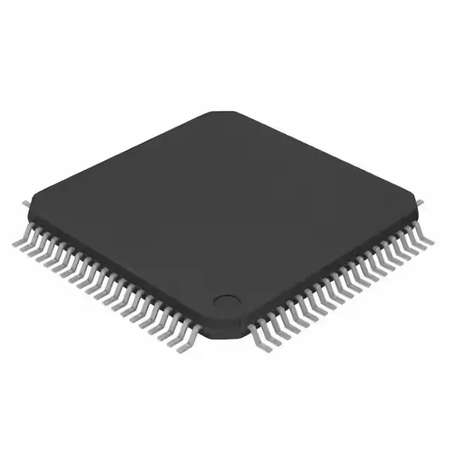
NXP LPC17xx series, ARM Cortex-M3 32-bit MCU at 100 MHz, 64KB flash, 16KB SRAM, 52 GPIO, CANbus/I2C/SPI/USB/SSP, 6x12b SAR ADC, internal oscillator, 2.4–3.6V supply, -40 to 85°C operating temperature, supplied in tray of 80-LQFP (12x12 mm).
- 100% new & originalTraceable channels only — no refurbs, no pulls, no remarked parts.
- Date & lot codes on quoteStated per line before you commit; label photos on request.
- MSL-compliant ESD packingMoisture-sealed bags with indicator cards; reels photo-verified.
- PayPal buyer protectionPay by T/T, PayPal or Payoneer — card payments covered end to end.
Specifications
| Parameter | Value |
|---|---|
| Series | LPC17xx |
| Mounting type | Surface Mount |
| Oscillator type | Internal |
| Program memory type | FLASH |
| Voltage - supply (Vcc (Vdd)) | 2.4V ~ 3.6V |
| Operating temperature | -40°C~85°C(TA) |
| Speed | 100MHz |
| Package | Tray |
| RAM size | 16K x 8 |
| Core size | 32-Bit Single-Core |
| Peripherals | Brown-out Detect/Reset, DMA, Motor Control PWM, POR, PWM, WDT |
| Connectivity | CANbus, I²C, IrDA, Microwire, SPI, SSI, SSP, UART/USART, USB |
| Number of i (O) | 52 |
| Core processor | ARM® Cortex®-M3 |
| Case | 80-LQFP |
| Data converters | A/D 6x12b SAR |
| Program memory size | 64KB (64K x 8) |
Frequently asked questions
Does the LPC1752FBD80K ship with a bootloader already programmed, or do I need to provision SWD/JTAG on first power-up?
Fresh units do not ship with user code preloaded. The device does carry a UART0 ISP bootloader that is active on the entry pin strap, so SWD/JTAG provisioning is not strictly required if the design routes the UART0 pins and uses the bootloader entry sequence. If SWD is the only update path on the panel, provision it at first power-up before field deployment.
I need to isolate a noisy ADC channel without a board re-spin — can I remap the 12-bit ADC pins in firmware on the LPC1752FBD80K?
Yes — the ADC channels are pin-muxed via the shared-function routing register, so firmware can remap the ADC function to different physical GPIO pins without hardware changes. The swap requires a firmware update and a power cycle to latch the mux configuration. A fully failed ADC input cannot be bypassed this way, but a noisy or drifting channel can be migrated to a cleaner physical pin and the original pin re-purposed.
I am running the 80-LQFP at 70 °C forced-air ambient in a DIN enclosure — do I need to worry about the internal oscillator accuracy?
The internal RC oscillator is characterized across the full -40 to 85 °C operating range, and the worst-case error band is wider than the nominal frequency. If the design relies on UART baud-rate tolerance or PWM edge timing derived from the internal clock, budget for the full datasheet error band rather than the nominal frequency. Any precision timing requirement should use an external crystal.
The LPC1752FBD80K is showing 3.3 V nominal GPIO — do I need level shifters to pair it with 24 V digital-input safety modules?
External level-shifting is required. Standard GPIO on the LPC1752 is not 24 V tolerant. NXP publishes reference schematics for voltage boundary interfacing; the common approach is a resistor-divider or a buffered level-shifter IC between the 3.3 V MCU output and the 24 V input module. Standard GPIO cannot be wired directly to 24 V logic levels without overstress damage.