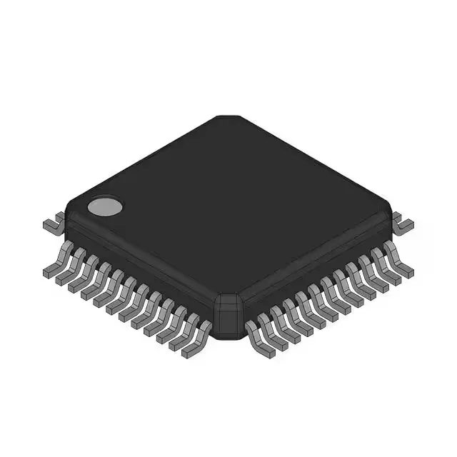
NXP LPC1549JBD48151 — ARM Cortex-M3 MCU, 72MHz, 256KB Flash, 48-LQFP
NXP LPC15xx series ARM Cortex-M3 MCU; 72MHz internal oscillator; 256KB Flash / 36KB RAM / 4KB EEPROM; 16x12-bit ADC, CANbus, USB, SPI/I²C/UART; 30 I/O in 48-LQFP (7x7mm); 2.4V–3.6V supply; -40°C to 105°C; bulk pack.
- 100% new & originalTraceable channels only — no refurbs, no pulls, no remarked parts.
- Date & lot codes on quoteStated per line before you commit; label photos on request.
- MSL-compliant ESD packingMoisture-sealed bags with indicator cards; reels photo-verified.
- PayPal buyer protectionPay by T/T, PayPal or Payoneer — card payments covered end to end.
Specifications
| Parameter | Value |
|---|---|
| Series | LPC15xx |
| Mounting type | Surface Mount |
| Oscillator type | Internal |
| Program memory type | FLASH |
| Voltage - supply (Vcc (Vdd)) | 2.4V ~ 3.6V |
| Operating temperature | -40°C~105°C(TA) |
| Speed | 72MHz |
| Package | Bulk |
| RAM size | 36K x 8 |
| Core size | 32-Bit Single-Core |
| EEPROM size | 4K x 8 |
| Peripherals | Brown-out Detect/Reset, DMA, POR, PWM, WDT |
| Connectivity | CANbus, I²C, SPI, UART/USART, USB |
| Number of i (O) | 30 |
| Core processor | ARM® Cortex®-M3 |
| Case | 48-LQFP |
| Data converters | A/D 16x12b |
| Program memory size | 256KB (256K x 8) |
Frequently asked questions
Does the LPC1549JBD48151 require an external crystal for the 72MHz clock?
No — the internal oscillator runs at 72MHz without an external crystal. Designs needing tighter USB timing accuracy than the internal RC provides should add an external crystal on the dedicated oscillator pins; verify the calibrated accuracy specification in the full NXP datasheet before removing that option from the BOM.
Can the 16x12-bit ADC run simultaneously with USB and CANbus without starving the DMA pool?
The DMA controller handles independent conversion-result transfers to the 36KB SRAM, and the CAN and USB peripheral DMA paths do not share the same bus arbitration cycle. The constraint is not hardware — it is firmware allocation of the 36KB RAM pool between concurrent ADC, CAN, and USB DMA buffers. Board-level integrators manage that at the HAL configuration level.
Is the 48-LQFP pinout of the LPC1549JBD48151 a drop-in for other LPC15xx variants in the same package?
The 48-LQFP foot-print is consistent across the LPC15xx family at the package level, but pin function allocation (which pin carries which peripheral signal) can differ by MPN. Treat any variant other than the exact MPN as requiring a schematic pin-assignment check and layout review before production substitution.