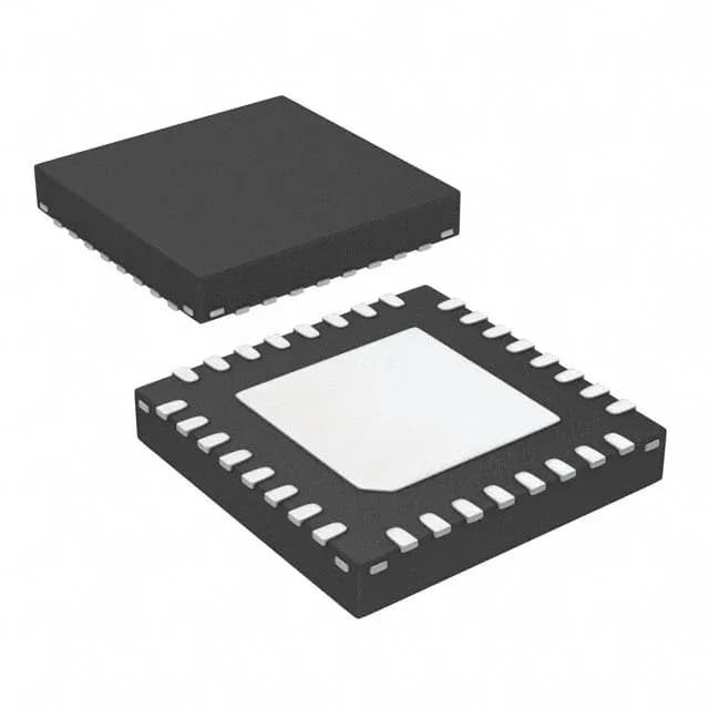
NXP LPC1317FHN33,551 — ARM Cortex-M3 MCU, 72MHz, 64KB Flash, 32-VQFN
NXP LPC13xx series ARM Cortex-M3 MCU, LPC1317FHN33,551, 72MHz core, 64KB Flash/10KB RAM, 2–3.6V supply, 26 I/O, 8×12-bit ADC, SPI/SSP/I²C/UART, internal oscillator, 32-VQFN exposed pad (7×7mm), -40°C to 85°C, Active.
- 100% new & originalTraceable channels only — no refurbs, no pulls, no remarked parts.
- Date & lot codes on quoteStated per line before you commit; label photos on request.
- MSL-compliant ESD packingMoisture-sealed bags with indicator cards; reels photo-verified.
- PayPal buyer protectionPay by T/T, PayPal or Payoneer — card payments covered end to end.
Specifications
| Parameter | Value |
|---|---|
| Series | LPC13xx |
| Mounting type | Surface Mount |
| Oscillator type | Internal |
| Program memory type | FLASH |
| Voltage - supply (Vcc (Vdd)) | 2V ~ 3.6V |
| Operating temperature | -40°C~85°C(TA) |
| Speed | 72MHz |
| Package | Tray |
| RAM size | 10K x 8 |
| Core size | 32-Bit Single-Core |
| EEPROM size | 4K x 8 |
| Peripherals | Brown-out Detect/Reset, POR, WDT |
| Connectivity | I²C, Microwire, SPI, SSI, SSP, UART/USART |
| Number of i (O) | 26 |
| Core processor | ARM® Cortex®-M3 |
| Case | 32-VQFN Exposed Pad |
| Data converters | A/D 8x12b |
| Program memory size | 64KB (64K x 8) |
Frequently asked questions
Is the 64KB Flash / 10KB RAM on the LPC1317FHN33,551 compatible with an existing LPC13xx CMSIS pack without a linker-script rebuild?
LPC1317 is the base product number (LPC1317) within the LPC13xx series. CMSIS packs are series-targeted, so a pack built for the LPC13xx family targets the ARM Cortex-M3 core and the on-chip peripheral set — the linker script defines the memory map. A linker-script rebuild is typically required when moving between members with different Flash or RAM sizes, because the region sizes in the scatter file must match the physical memory. Confirm the scatter file's FLASH and RAM region lengths match the 64KB/10KB partition before flashing without changes.
Does the 8×12-bit ADC on the LPC1317FHN33,551 require an external reference pin, and does it consume I/O from the 26-pin allocation?
The ADC channels are muxed onto the 26 general-purpose I/O pins — meaning the eight converter inputs are a subset of those pins, not additional. Whether VDD serves as the reference or a dedicated reference pin is used depends on the pin-mux configuration chosen in firmware; the spec table does not isolate the ADC reference architecture from the I/O allocation.