It is organized as 64 M x 8 bits and clocks at 200 MHz, designed for high-throughput code-shadowing or data-logging in systems that need fast random read and execute-in-place (XiP) capability.
At 200 MHz the Xccela Bus delivers significantly higher read throughput than the 133 MHz SPI interface on the older MT25QU256ABA1EW7-0SIT. That extra margin matters when the host MCU or FPGA is starving for code fetch bandwidth — you can sustain back-to-back reads without wait states on a well-laid-out board. The trade-off is that the Xccela interface is not pin-compatible with SPI; the PCB layout must follow Micron's Xccela routing guidelines to keep signal integrity at that clock rate.
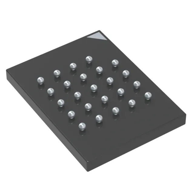
Housed in a 24-TBGA (24-T-PBGA 6x8 mm), surface-mount only. The 6x8 mm ball grid array is compact for a 512 Mbit NOR — check your PCB land pattern against the supplier package drawing before layout. No through-hole option exists.