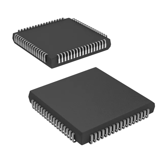
The Microchip (formerly Actel) A40MX02-FPLG68 is a nonvolatile, flash-based FPGA from the MX family, integrating 3000 gates and 57 user I/O in a 68-lead PLCC package with J-leads. It operates from either a 3V–3.6V or a 4.75V–5.25V supply rail, making it one of the few small FPGAs that can sit directly on a legacy 5V bus without level translation.
Dual supply — 3.3V and 5V compatibility
The A40MX02-FPLG68 accepts two separate supply ranges: 3V to 3.6V and 4.75V to 5.25V. This means the same device can interface with 3.3V-core microcontrollers and 5V peripheral logic without external voltage translators. For a BOM that mixes a 5V backplane with a 3.3V FPGA, this part eliminates a level-shifter IC and its associated board area.
3000 gates and 57 I/O — sizing the logic
With 3000 gates, this FPGA is sized for small-scale glue logic: address decoding, bus arbitration, state-machine control, or simple data muxing. The 57 I/O are enough to capture a 16-bit data bus plus control signals, but not for a full memory controller or video interface. If your design needs more than 3000 gates, the MX family offers the A40MX04 with 6000 gates and 69 I/O in a larger PLCC84 package.
The 68-PLCC (J-lead) package measures 24.23 mm per side and is surface-mountable. PLCC sockets are available for prototyping or field-replaceable modules. The J-lead form factor is robust for hand-soldering rework, and the 68-lead count keeps the footprint manageable on a two-layer board.
For dual-sourcing or a drop-in upgrade with more logic, the A40MX04-PLG84 (6000 gates, 69 I/O, PLCC84) is a pin-compatible step within the same MX family — same supply ranges, same programming interface.