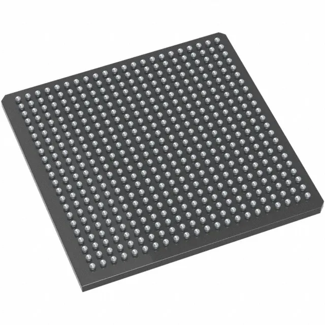
ProASIC3 FPGA with 1M gates and 300 I/O
The Microchip A3P1000-FGG484I is a nonvolatile flash-based FPGA from the ProASIC3 family, offering 1,000,000 system gates and 300 user I/O in a 484-ball FBGA package. The 1.425 V core supply simplifies the power rail — no separate VCCAUX or VCCPLL rails to sequence. On-chip 147456 bits of RAM support moderate FIFO and buffer needs without external SRAM.
Rated for junction temperature from -40°C to 100°C, this industrial-grade variant suits outdoor telecom cabinets, motor-drive control boards, and factory-floor logic that sees thermal cycling. The flash-based configuration is live at power-up — no external configuration memory or boot time, which matters in applications where the FPGA must be operational within milliseconds of supply rail stabilisation.
The ProASIC3 family has broad installed base and Microchip continues to support it for industrial and aerospace programs that require long design-in windows. No official second-source or direct replacement is listed — the flash FPGA architecture is proprietary to Microchip, so the BOM carries single-source risk.
Package and board-level considerations
484-ball FBGA on 1.0 mm pitch — the 300 I/O break out across the full ball field, so a four-layer PCB with buried vias is the practical minimum for fan-out.
What the 1.425 V core and 300 I/O mean for the BOM
The single 1.425 V core rail eliminates the need for a multi-output regulator — a single LDO or buck converter at 1.5 V with 3% accuracy covers the tolerance. The 300 I/O count supports wide parallel buses (e.g., 32-bit data + address to an external SRAM or ADC array) with room for control and status signals. Each I/O is programmable to multiple standards, but the bank voltage must match the interface — plan the PCB split planes accordingly.