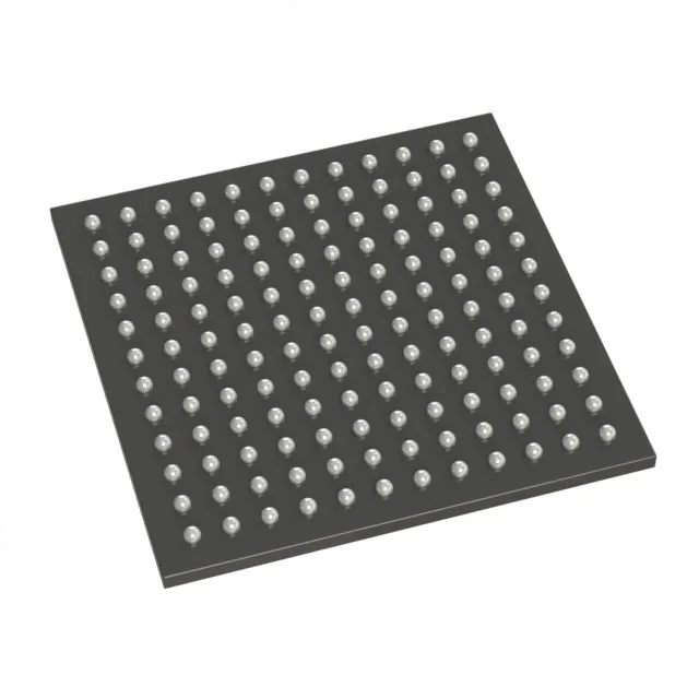
1M-gate ProASIC3 FPGA in 144-ball FBGA
The Microchip A3P1000-FG144I is a nonvolatile flash-based FPGA from the ProASIC3 family, offering 1 million system gates with 147456 bits of embedded RAM in a 144-ball FBGA package. It provides 97 user-configurable I/O pins and operates from a single 1.425 V core supply, simplifying the power delivery network compared to multi-rail FPGAs.
Flash FPGA: instant-on, no external boot memory
Because the configuration is stored in on-chip flash cells, the A3P1000-FG144I powers up and is operational in microseconds — no external SPI flash or configuration PROM is needed, and there is no configuration bitstream to manage during production. The 147456 bits of total RAM are distributed as block RAM across the fabric, sized for FIFO buffers, small packet caches, or coefficient storage in DSP chains. With 1 million system gates, this part fits medium-density glue logic consolidation, display controllers, or sensor fusion pre-processing — not the multi-million-gate class of a Kintex or Stratix, but a solid fit where deterministic timing and single-chip operation matter.
Industrial temperature and supply margins
Core supply is 1.425 V nominal — a clean 1.5 V rail with 5% tolerance keeps the core within spec; the I/O banks tolerate 3.3 V, 2.5 V, and 1.8 V standards, though the exact Vccio assignments depend on the bank mapping in the Libero design suite. The 144-ball FBGA footprint uses a 0.80 mm ball pitch — a 4-layer PCB with via-in-pad or microvias is the practical floor for fan-out; two-layer boards will struggle to route all 97 I/O plus power and ground.
The ProASIC3 family has been in production for over a decade; the flash process is mature, and Microchip continues to support it alongside the newer IGLOO2 and PolarFire families for designs that need the instant-on, single-chip flash architecture.