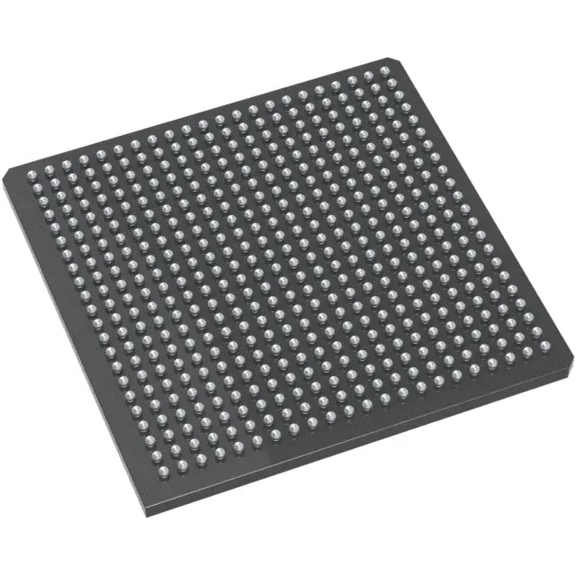
Microchip Technology A2F500M3G-FGG484I — FPGA / CPLD & Programmable Logic

A2F500M3G-FGG484I SmartFusion MCU+FPGA, 80MHz, 500K gates

MPNA2F500M3G-FGG484I
Active

Microchip SmartFusion series A2F500M3G-FGG484I, ARM Cortex-M3 MCU + ProASIC3 FPGA, 80 MHz, 512KB flash, 500K gates, 11520 D-Flip-Flops, 41 MCU + 128 FPGA I/O, -40°C to 100°C, 484 FBGA.

$104.31Ref. price · indicative, final on quote
StockContact for availability
MOQ1 pcs
  • 100% new & originalTraceable channels only — no refurbs, no pulls, no remarked parts.
  • Date & lot codes on quoteStated per line before you commit; label photos on request.
  • MSL-compliant ESD packingMoisture-sealed bags with indicator cards; reels photo-verified.
  • PayPal buyer protectionPay by T/T, PayPal or Payoneer — card payments covered end to end.

Specifications

A2F500M3G-FGG484I Technical Specifications
ParameterValue
SeriesSmartFusion®
Frequency80 MHz
Operating temperature high-40°C to 100°C (TJ)
Cpu_coreARM® Cortex®-M3
Frame_size512KB
Fuse_speed80 MHz
ArchitectureMCU, FPGA
ConnectivityEBI/EMI, Ethernet, I²C, SPI, UART/USART
Package_typeTray
Number of i (O)MCU - 41, FPGA - 128
Product_statusActive
Peripheral_typesDMA, POR, WDT
Primary attributesProASIC®3 FPGA, 500K Gates, 11520 D-Flip-Flops

Product details

Hybrid MCU-FPGA on a single die

The Microchip A2F500M3G-FGG484I is a SmartFusion series device that integrates an ARM Cortex-M3 processor core running at 80 MHz with a ProASIC3 FPGA fabric rated at 500K gates and 11520 D-Flip-Flops. This is not a package-on-package stack — the MCU and FPGA share the same die with an internal bus bridge, so the latency between the processor and the programmable logic is deterministic and measured in single-digit clock cycles. The FPGA side is a flash-based ProASIC3 array — no configuration PROM needed, it powers up live.

I/O budget and package constraints

The 484-ball FBGA package breaks out 41 dedicated MCU I/O and 128 FPGA I/O. That 41+128 split is fixed — the MCU I/O are on fixed pins and cannot be reassigned to the FPGA fabric. The FPGA I/O are banked and can be configured to 1.2 V, 1.5 V, 1.8 V, 2.5 V, or 3.3 V per bank, which matters when the FPGA side interfaces to sensors at one voltage and a memory bus at another. The 484-ball array is a 23×23 ball grid with 1.0 mm pitch — four-layer board minimum for fan-out, though six layers are typical when the Ethernet PHY and external memory are on the same board.

Rated for junction temperature from -40°C to 100°C, this part sits in the industrial operating band. It is suited for motor drives, PLC I/O modules, Ethernet gateways, and instrumentation that lives in a panel or cabinet where ambient air can hit 70°C and the die runs another 30°C above that. Not rated for automotive under-hood (125°C junction is the typical threshold there), but fine for most factory-floor and outdoor telecom enclosures.

Lifecycle and supply position

This is a current-production part from Microchip, not a legacy or sunset line.

Frequently asked questions

What are the complete specifications of A2F500M3G-FGG484I including CPU speed, FPGA size, and I/O?

The FPGA fabric is a ProASIC3 array rated at 500K gates with 11520 D-Flip-Flops. There are 41 dedicated MCU I/O and 128 FPGA I/O, for a total of 169 user-accessible I/O.