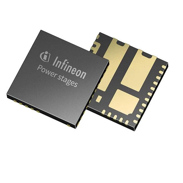
Infineon Technologies TDA21490AUMA1 — Analog & Data Acquisition

Infineon TDA21490AUMA1 OptiMOS Power Stage

MPNTDA21490AUMA1
End of Life

Infineon Technologies OptiMOS™ power stage driver, TDA21490AUMA1, N-Channel MOSFET, non-inverting, dual independent channels, 90A peak source / 70A sink, 4.25V-16V supply, -40°C to 125°C, surface mount 39-PowerVFQFN, PG-IQFN-39.

$6.95Ref. price · indicative, final on quote
Packaging39-PowerVFQFN
RoHSROHS3 Compliant
SeriesOptiMOS™
Sourced new & surplus through independent channelsAuthenticity-screened · ESD-safe packingListing updated Aug 2026

Specifications

TDA21490AUMA1 specifications
ParameterValue
SeriesOptiMOS™
Gate typeN-Channel MOSFET
Input typeNon-Inverting
Channel typeIndependent
MountingSurface Mount
Voltage4.25V ~ 16V
Current - peak output (Source, sink)90A, 70A
Operating temperature-40°C ~ 125°C (TJ)
PackageTape & Reel (TR); Cut Tape (CT)
Case39-PowerVFQFN
Number of drivers2
Driven configurationHigh-Side or Low-Side

Product details

Power stage driver with 90 A peak drive capability

The TDA21490AUMA1 is an Infineon OptiMOS™ power stage driver that integrates a dual N-channel MOSFET gate driver with a peak output capability of 90 A source and 70 A sink. This drive strength handles the gate charge of large synchronous rectifier MOSFETs in high-current voltage regulator modules, keeping switching losses in check at multi-hundred-kHz frequencies.

Dual-channel, high-side or low-side configuration

Two independent driver channels with non-inverting input support high-side or low-side driven configuration, making the TDA21490AUMA1 suitable for synchronous buck converters, half-bridge stages, and dual-phase power stages without external level shifting. The N-channel MOSFET gate type means the driver sources current to turn on the external FET and sinks current to turn it off, with the 90 A / 70 A peak rating ensuring fast rise and fall times even with high gate charge loads.

The compact footprint suits dense power supply layouts where multiple phases share a small board area, but the thermal pad requires a via array to the inner ground plane to keep junction temperature below 125°C under continuous 90 A peaks.

Frequently asked questions

What is the peak output current of TDA21490AUMA1?

The TDA21490AUMA1 delivers 90 A peak source current and 70 A peak sink current, making it suitable for driving high-gate-charge MOSFETs in high-current voltage regulator modules.

What supply voltage range does TDA21490AUMA1 support?

The supply voltage range is 4.25 V to 16 V, covering standard 5 V and 12 V gate drive rails commonly used in automotive and industrial power stages.