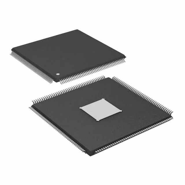
176-pin LQFP with exposed pad — thermal and layout considerations
The TC265D40F200WBCKXUMA1: The pad carries the bulk of the junction-to-board heat path — the 0.5 mm pitch perimeter leads alone cannot sink the full dissipation of a 200 MHz dual-core TriCore running both cores flat out. The 176-lead count with 112 I/O means at least four signal layers are advisable for fan-out — two-layer boards will struggle to route the peripheral set.
Dual-core TriCore architecture — safety and performance domains
Two 32-bit TriCore cores running at 200 MHz each give the TC265D40F200WBCKXUMA1 the headroom to split a real-time control loop from a safety-monitoring task without a second chip. One core can execute the application control algorithm while the other runs the diagnostic software layer — a common pattern in ASIL-B and ASIL-D systems. The 2.5 MB on-chip flash and 240 KB RAM cover most powertrain, transmission, and ADAS sensor-fusion firmware images without external memory. The 96 KB EEPROM block stores calibration and fault-log data that survives power cycles.
Vehicle-domain connectivity — Ethernet, FlexRay, CAN, PSI5, SENT
The peripheral set covers every major automotive serial bus: CANbus (multiple nodes), FlexRay for deterministic chassis control, Ethernet for high-bandwidth diagnostics or OTA updates, LINbus for low-cost body nodes, and the sensor-specific PSI5 and SENT interfaces for airbag and pressure-sensor arrays. The HSSL (High-Speed Serial Link) provides a 80 Mbit/s point-to-point channel between AURIX devices in a multi-MCU system. The 50-channel 12-bit ADC and three sigma-delta converters can sample current, voltage, and position signals from multiple sensors simultaneously — enough analog front-end for a six-phase motor controller reading phase currents, DC bus voltage, and resolver feedback on the same device.
Active lifecycle and sourcing posture
Infineon lists the TC265D40F200WBCKXUMA1 as Active (current production) with ROHS3 compliance. Sourced through authorized and independent distribution channels; pricing and lead time are confirmed at RFQ against the BOM quantity.