650 V CoolMOS™ — what this N-channel MOSFET brings to the power stage
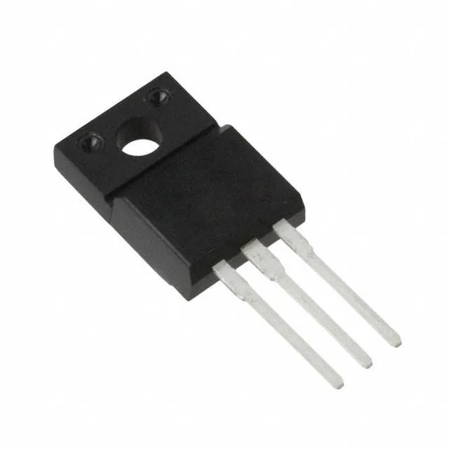
The SPA20N65C3XKSA1: The full-pack (isolated) TO-220-3 variant eliminates the need for an insulating washer between the tab and heatsink, simplifying assembly in grounded-heatsink designs.
The wide temperature window also provides thermal headroom for derating in high-current, high-frequency switching stages.
NRND status — plan the replacement now
Infineon lists this part as Not Recommended for New Designs (NRND). That means it is still available through existing inventory and last-time-buy windows, but the manufacturer will not guarantee long-term production. For new BOM lines or a second-source qualification, the buyer should identify a pin-compatible successor in the CoolMOS™ family — the C3 series has been superseded by later generations that offer lower Rds(on) and faster switching. The SPA20N65C3XKSA1 remains a valid replacement for the older SPA20N65C3 in service and repair applications, provided the date codes and thermal interface match.
Specs that drive the design decision
The 650 V drain-source rating provides a 1.6× margin over a nominal 400 VDC bus (typical PFC output), leaving room for switching overshoot and line transients. The 190 mOhm Rds(on) at 10 V gate drive sets the conduction loss target: at 13.1 A drain current, expect roughly 33 W dissipation in the channel alone — the 34.5 W package power limit means the heatsink design is critical. Gate charge of 114 nC at 10 V dictates the driver's peak current capability; a standard 1 A gate driver will slew the gate in about 114 ns, acceptable for switching frequencies up to 100 kHz. Input capacitance of 2400 pF at 25 V Vds influences the drive loop and contributes to switching losses.