650 V / 15 A CoolMOS™ — what this N-channel MOSFET brings to a PFC or LLC stage
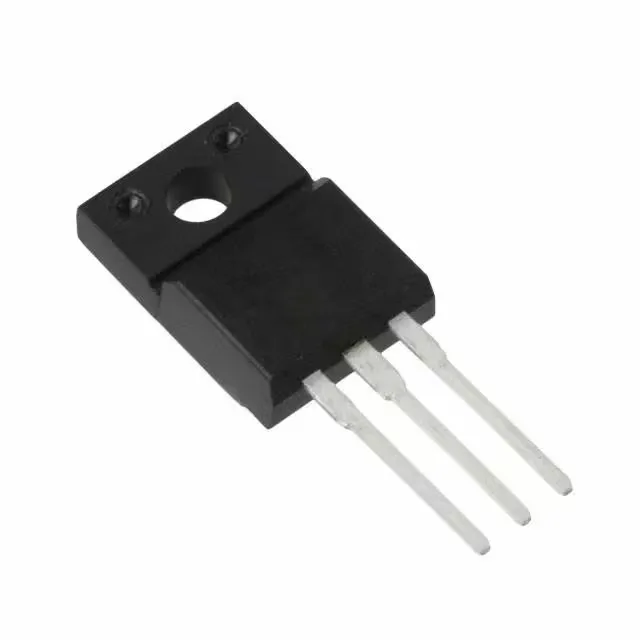
The SPA15N65C3XKSA1: It comes in a TO-220-3 Full Pack through-hole package (PG-TO220-3-31), which means the back of the package is fully isolated — no insulating pad needed against the heatsink, a real assembly-time saver in high-voltage offline supplies. The 34 W power dissipation ceiling (Tc) means the thermal path to the heatsink needs attention at high switching frequencies.
The SPA15N65C3XKSA1 is marked obsolete by Infineon. In a shortage cycle this part would command a spot premium because the CoolMOS™ C3 generation has wide installed base in PFC and LLC designs; right now the procurement move is to qualify a cross — either a later CoolMOS™ C7 or P7 device in the same TO-220 Full Pack footprint, or a pin-compatible competitor like an ST STF15N65M5 or an On Semi NTP15N65. The datasheet is still available from Infineon's archive, but no new production is running.
At 280 mOhm maximum with 9.4 A drain and 10 V gate drive, the conduction loss at 9.4 A is about 25 W — which eats into the 34 W package power limit. That means the heatsink design is not optional; the Full Pack case helps with isolation but the thermal resistance junction-to-case still needs a good thermal interface to keep junction temperature under 150°C. The 3.9 V maximum gate threshold at 675 µA drain current is typical for CoolMOS™ — the device turns on fully at 10 V, but the threshold is low enough that a gate-drive undervoltage lockout set above 8 V is prudent to avoid linear-mode operation during startup.