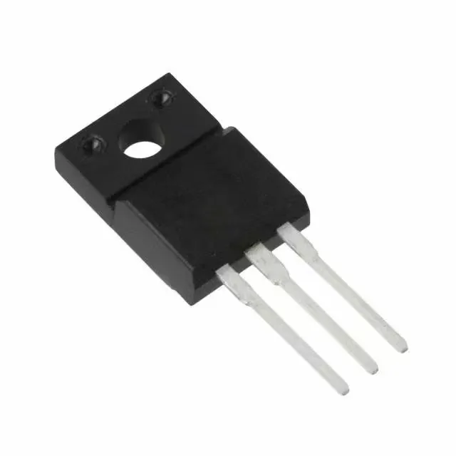
The SPA11N80C3XKSA1: The TO-220 Full Pack package (PG-TO220-3-31) has a fully isolated metal tab — no insulating pad or washer needed between the device and the heatsink, which simplifies assembly and improves thermal coupling.
450 mOhm Rds(on) and 85 nC gate charge — conduction and switching
At 11 A full load, conduction loss is about 5.4 W at the hot junction — within the 34 W power dissipation rating, but thermal design should budget for the Rds(on) increase at 150°C junction (roughly double the 25°C value). Gate charge totals 85 nC at 10 V, which is moderate for an 800 V device; a gate-drive IC capable of sourcing at least 1 A peak will keep switching transitions clean in a 100 kHz PFC stage. Input capacitance is 1600 pF at 100 V drain-source, giving a figure of merit (Rds(on) × Qg) around 38 mOhm·nC — competitive for this voltage class. The gate threshold voltage maximum is 3.9 V at 680 µA drain current, and the recommended drive voltage is 10 V for minimum Rds(on). A logic-level 5 V gate signal will not fully enhance this device — the design needs a 10 V rail or a bootstrap supply for the gate driver.
Through-hole mounting and thermal interface
The TO-220 Full Pack package suits through-hole mounting on a PCB or direct connection to a heatsink via the mounting hole. The isolated tab eliminates the need for a silicone pad or mica washer, reducing thermal resistance by about 0.5°C/W compared to a standard TO-220 with an insulator. In practice, derate based on the maximum junction temperature of 150°C and the expected case temperature in the enclosure.
Temperature range and application environments
The 800 V drain-source rating provides margin for universal-input AC-DC converters (85–265 VAC) where the rectified DC bus peaks near 375 V, and for PFC stages that switch at 400 V DC bus.