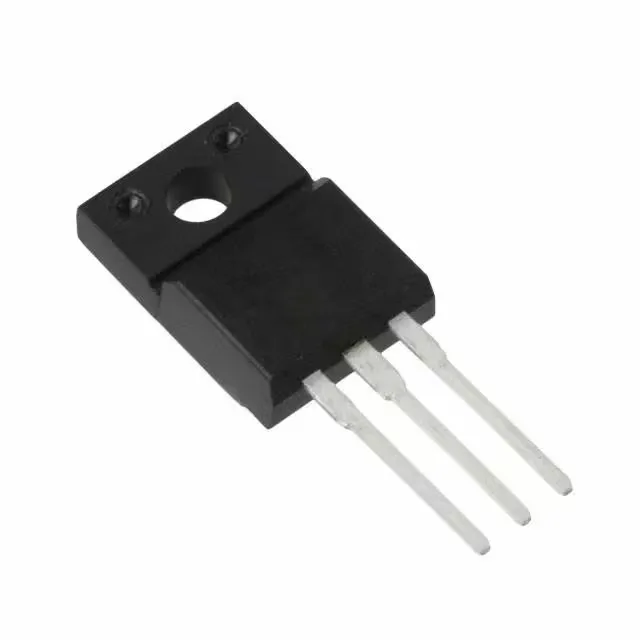
800 V CoolMOS for offline flyback and PFC stages
The SPA04N80C3XKSA1: Built on Infineon's CoolMOS technology, it delivers a maximum on-resistance of 1.3 Ohm at 10 V gate drive with 2.5 A drain current — the figure you use for conduction loss budgeting in the steady-state operating point.
Rds(on) and gate drive — sizing the conduction and switching loss
The 1.3 Ohm maximum Rds(on) is specified at 10 V gate-source with 2.5 A drain current. At reduced gate drive — say 4.5 V from a logic-level output — the on-resistance roughly doubles, so this part expects a 10 V rail for the gate driver to hit the rated conduction loss. The gate threshold voltage maximum is 3.9 V at 240 µA drain current, which means the device is fully enhanced at 10 V but marginal below 5 V. At 100 kHz switching frequency, the gate drive power requirement sits around 31 mW — well within a standard gate driver IC's capability.
Infineon has announced end-of-life for this CoolMOS variant, and the final ordering window is closing. New designs should evaluate the current-generation CoolMOS replacement — parts in the same voltage and current class offer lower Rds(on) and improved switching performance.
Through-hole mounting and thermal interface
The TO-220 Full Pack package is a through-hole device that mounts into a standard pitch hole pattern on the PCB. Maximum power dissipation is 38 W at case temperature, which requires a heatsink for any continuous load above a few watts. The PG-TO220-3-31 variant has the standard three-lead form factor with the drain on the center lead.