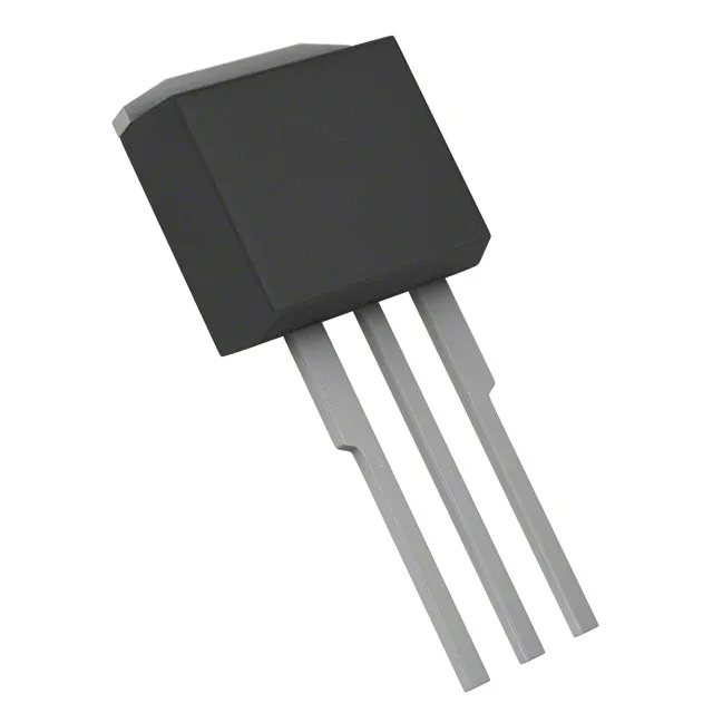
60 V N-channel power switch in TO-262
Total gate charge of 65 nC at 10 V means a moderate gate-drive current — about 6.5 mA at 100 kHz switching frequency — so a standard driver IC handles it without excessive dissipation.
Thermal and drive margins for the TO-262 build
Maximum power dissipation is 92 W at the case temperature — the TO-262 package's large copper tab couples heat into the heatsink or PCB plane, but the 175 °C junction limit means the thermal resistance from junction to case must be kept below about 1.6 °C/W for full current. Input capacitance is 1690 pF at 25 V drain-source, which together with the 65 nC gate charge defines the switching loss profile — the driver must source and sink enough peak current to charge and discharge this capacitance within the dead-time budget.