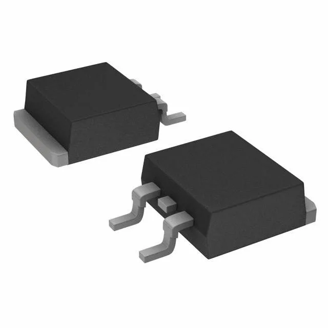
100 V, 33 A, 44 mOhm — the power-switch parametric envelope
The IRF540NSPBF is an N-channel enhancement-mode MOSFET from Infineon's HEXFET series, built on a planar stripe-gate process. At 16 A load, I²R loss is about 11.3 W at the hot junction — the D2PAK tab must be soldered to a sufficient copper area on the PCB to keep the junction below 175°C.
Total gate charge is 71 nC at 10 V. A gate driver sourcing 1 A can charge the gate in about 71 ns, but the practical switching speed is limited by the driver's peak current and the gate loop inductance. If the PWM controller or driver only outputs 5 V, the on-resistance will be higher than the 44 mOhm spec — budget for the increase from the typical Rds(on) vs Vgs curve.
D2PAK footprint and thermal path
The ±20 V maximum gate-source voltage is a hard limit; a zener clamp on the gate is cheap insurance against ringing.