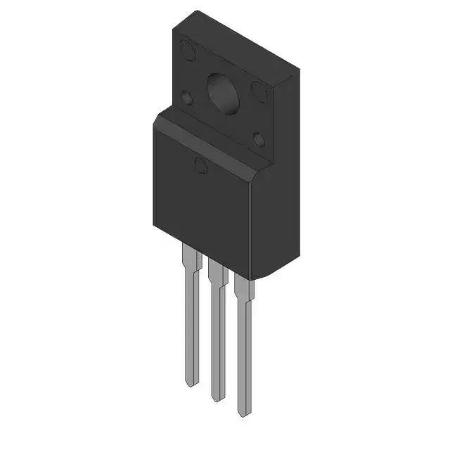
Package and board-fit — TO-220 through-hole
The IRF3709PBF comes in a through-hole TO-220 package, shipped in bulk tubes. That means the leads are thick enough to take a soldering iron or a socket without worrying about lifted pads — a rework-friendly part that survives a hot-air desoldering cycle as long as you keep the junction below 150°C (the max operating junction temp per the spec). The three-lead layout is standard TO-220: gate, drain (tab), source. Pin 1 is the gate — orient it by the tab side before you solder. The tab is the drain, so if you're bolting it to a heatsink, that sink is at drain potential; insulate it or keep the chassis isolated.
On-resistance and gate drive — what the numbers mean for your circuit
Rds(on) is 9 mOhm max at Vgs=10 V, Id=15 A. That's the on-resistance you design the conduction loss around at full gate drive. At 15 A, the dissipation is I²R = 2.0 W — well within the 3.1 W total power rating, but only if the junction stays under 150°C. The 9 mOhm figure is at 25°C junction; expect it to roughly double at 125°C, so budget for the hot resistance in your thermal loop. Gate threshold is 3 V max at 250 µA drain current. For full conduction, drive the gate to 10 V. The ±20 V Vgs rating gives headroom against ringing on long gate traces — you won't blow the oxide with a 12 V gate drive rail.
Switching performance — 90 A peak, 41 nC gate charge
The 90 A switching current is a pulse rating, not continuous DC. Use it for motor inrush, capacitor charging, or load-switch transients. The continuous drain current is derated by package and temperature — the TO-220 body limits steady-state current to about 30-40 A with adequate heatsinking, but the silicon can handle the peak. Gate charge Qg is 41 nC at Vgs=5 V. That's moderate — a typical gate driver with 1 A peak output can switch it in about 40 ns. For a 100 kHz SMPS, the gate drive power is Qg × Vgs × f = 41 nC × 5 V × 100 kHz = 20.5 mW, negligible. The 0.0027 µF input capacitance (Ciss) is consistent with a 90 A-class die — your driver sees a capacitive load of about 2.7 nF at the gate.