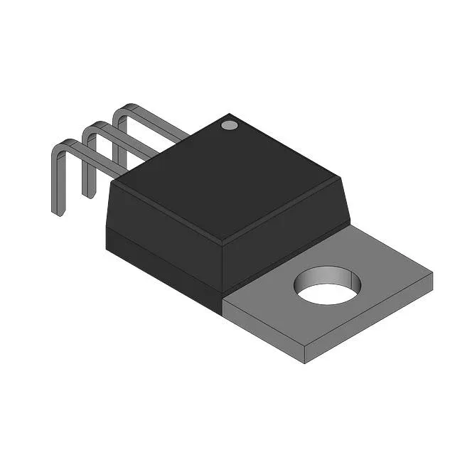
900 V CoolMOS — high-voltage switching for auxiliary and PFC stages
The 42 nC typical gate charge at 10 V and 1100 pF input capacitance at 100 V drain bias give a moderate switching speed suited for hard-switched topologies like flyback auxiliary supplies, two-switch forward converters, and power-factor correction stages where the 900 V margin buys headroom over 600 V or 650 V alternatives.
At reduced gate voltage the on-resistance climbs — the Vgs(th) max of 3.5 V at 460 µA means the device is fully enhanced by 10 V, but logic-level drive at 5 V will roughly double Rds(on) compared to the 10 V figure. For designs running from a 12 V or 15 V auxiliary rail the 10 V drive is straightforward; if the gate driver rail is lower, budget for higher conduction loss or select a part with lower threshold. The 33 W power dissipation ceiling at case temperature sets the thermal limit — with the TO-220 Full Pack's junction-to-case thermal path, a heatsink is required for any continuous load above a few watts.
Temperature range and package — where this part goes
The TO-220 Full Pack (PG-TO220 Full Pack) is a through-hole package with the backside tab fully encapsulated, so no mica washer or sil-pad is needed for isolation; the mounting screw directly clamps the package to the heatsink. This simplifies assembly and reduces BOM count, though the thermal resistance is slightly higher than a standard TO-220 with an external insulator.
For ongoing designs this means no supply discontinuity risk from obsolescence. If a second-source or pin-compatible alternative is needed, the CoolMOS family includes other 900 V devices in the same TO-220 Full Pack footprint — parametric differences in Rds(on) and current rating should be verified against the design's thermal and efficiency targets.