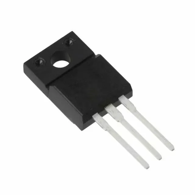
650 V CoolMOS — the isolated-package workhorse for offline power
This part belongs to Infineon's CoolMOS family, a mature high-voltage MOSFET platform optimised for hard-switching topologies like PFC boost stages, flyback converters, and LLC half-bridges in AC-DC power supplies rated up to several hundred watts.
NRND — plan the last-time-buy or evaluate a drop-in
For a BOM line already qualified, that means the window for last-time-buy orders is open but finite — Infineon will eventually issue an EOL notice with a final order date. New designs should target a currently-active CoolMOS sibling in the same voltage and package class. Sourcing through independent distribution remains viable for production support and bridge quantities, but the NRND flag should trigger a qualification plan for an alternative if volume production extends beyond the next 12–18 months.
The 650 V Vdss gives 15–20% margin on a 400 V DC bus (typical PFC output), which is comfortable for universal-input offline supplies. Gate charge of 32 nC at 10 V is moderate — a standard gate driver IC can switch it at 65–100 kHz without excessive driver dissipation. Input capacitance of 870 pF at 100 V Vds is low enough that the Miller plateau does not dominate the switching transition, but you still want a gate-drive resistor in the 10–22 Ω range to control dv/dt.
Package note: TO-220 Full Pack rework and mounting
The PG-TO220-3-111 Full Pack is a through-hole package with the mounting hole in the tab. That saves a BOM line and a manual assembly step. For rework, the plastic body is thicker than a standard TO-220, so it takes a bit longer to heat-soak the tab when desoldering; a 400°C iron with a wide tip works. The package is MSL 1, no bake required before reflow if the bag seal is intact.