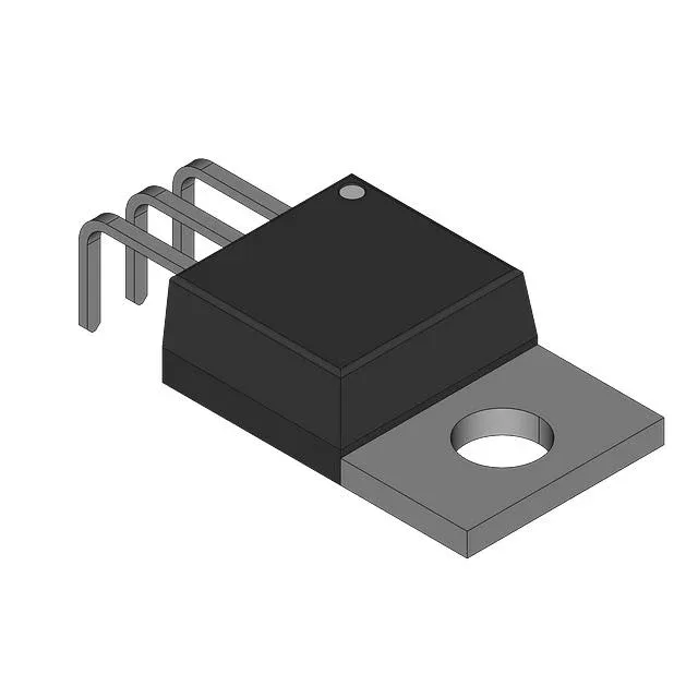
That 190 mOhm Rds(on) sets the conduction loss anchor for a PFC boost stage or flyback primary switch — at 7.3 A the dissipation sits at roughly 10 W, which the 34 W package limit can handle with a modest heatsink. In a real 85°C ambient with forced air, expect to derate to around 12–14 A continuous; the datasheet's safe operating area curve is the final arbiter for your switching frequency and duty cycle.
Gate drive and switching — 73 nC total gate charge
Total gate charge is 73 nC at 10 V Vgs, which is moderate for a 650 V, 190 mOhm device. A typical 1 A gate driver can charge the gate in about 73 ns, keeping switching losses manageable in a 100 kHz PFC. Input capacitance (Ciss) is 1620 pF at 100 V Vds — that's the load the gate driver sees during the Miller plateau. Pair it with a driver that can source and sink at least 1 A to avoid excessive turn-on/turn-off delay in hard-switched topologies.
The wide TJ range also gives headroom for transient overloads in automotive auxiliary converters (though this part is not AEC-Q101 qualified per the listing).