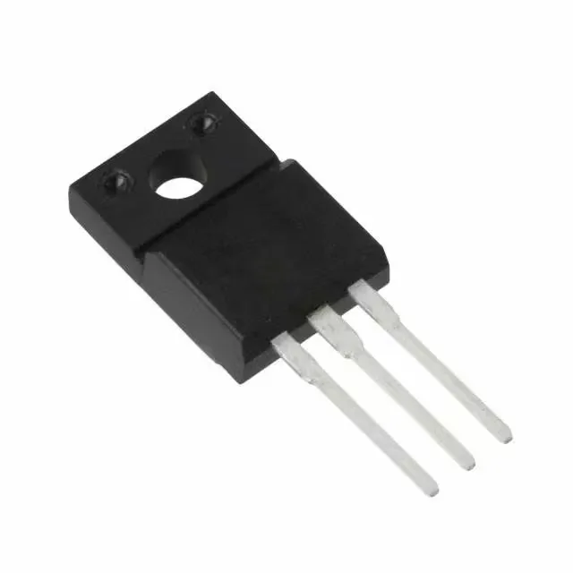
650 V CoolMOS — what this part was designed for
It was designed for high-efficiency power conversion in switched-mode power supplies, power factor correction stages, and flyback converters where the full-pack isolation simplifies heatsinking by eliminating the need for an insulating pad.
Key ratings that drive the design decision
The 650 V drain-source breakdown voltage sets the bus voltage ceiling — this part fits 380 V DC-link PFC stages and universal-input flybacks with margin. Gate charge of 86 nC at 10 V gives a sense of the drive energy per switching cycle — relevant when sizing the gate driver and estimating switching losses at frequency. Input capacitance of 2340 pF at 100 V Vds influences the drive current requirement and turn-on delay. The 34.7 W power dissipation ceiling at the case defines the thermal budget; the full-pack package conducts heat through the back tab, so a greased interface to a heatsink is the typical mounting.
This simplifies assembly and reduces thermal resistance in the mounting stack. The through-hole leads suit wave-solder or hand-solder rework.