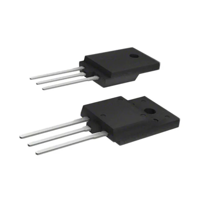
500 V N-channel in a thermally isolated package
Its 950 mOhm maximum on-resistance is specified at 1.2 A with a 13 V gate drive, which is the typical operating point for this device.
Switching losses and drive requirements
With a gate charge of 10.5 nC at 10 V, this part keeps the gate-drive energy low, which directly reduces losses in the driver stage and lets you push switching frequency higher than a higher-Qg part would allow. Input capacitance measures 231 pF at 100 V drain-source, confirming the light capacitive load.
Thermal budget for the full-pack design
Maximum power dissipation is 25.7 W at case temperature, but the Full Pack's higher thermal resistance means the junction-to-case path is the limiting factor — derate aggressively if the heatsink is small or airflow is restricted.
The part is in the CoolMOS CE series, a mainstream high-voltage MOSFET family with broad availability through independent distribution.