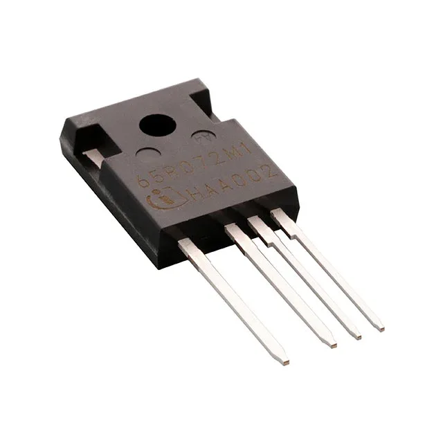
TO-247-4 Kelvin-source package — what it changes
The four-pin TO-247-4 includes a dedicated Kelvin source connection separate from the power source pin. This decouples the gate-drive loop from the high-current commutation loop, reducing parasitic inductance in the gate path. For a design that previously used a 3-pin TO-247 SiC MOSFET, switching to this package can lower gate-source voltage overshoot and allow tighter miller plateau control without adding external source resistors.
ROHS3 compliance covers EU and global regulatory requirements.
Gate drive and thermal considerations
The recommended drive voltage for achieving maximum Rds(on) is 18 V. Gate-source absolute maximum is +23 V and -5 V, so the driver must not exceed these limits during ringing. Maximum power dissipation is 96 W at case temperature, and the junction-to-case thermal path should be sized for the expected conduction and switching losses. The 744 pF input capacitance at 400 V is low for a 650 V SiC device, which reduces the gate-driver current requirement compared to a superjunction MOSFET of similar voltage and current rating.