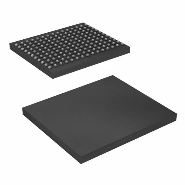
CY7C25422KV18-333BZXC Cypress 72Mbit QDR II+ SRAM, 333MHz, 165-FBGA
MPNCY7C25422KV18-333BZXC
Last Buy
Cypress CY7C25422KV18-333BZXC, 72Mbit synchronous QDR II+ SRAM, 333MHz, 1.7–1.9V, 2M x 36, 165-LBGA/FBGA, Surface Mount, Tray, 0°C to 70°C.
$228.2800Ref. price · indicative, final on quote
StockContact for availability
MOQ1 pcs
- 100% new & originalTraceable channels only — no refurbs, no pulls, no remarked parts.
- Date & lot codes on quoteStated per line before you commit; label photos on request.
- MSL-compliant ESD packingMoisture-sealed bags with indicator cards; reels photo-verified.
- PayPal buyer protectionPay by T/T, PayPal or Payoneer — card payments covered end to end.
Specifications
| Parameter | Value |
|---|---|
| Memory type | Volatile |
| Mounting type | Surface Mount |
| Voltage | 1.7V ~ 1.9V |
| Frequency | 333 MHz |
| Memory interface | Parallel |
| Operating temperature | 0°C ~ 70°C (TA) |
| Package | Tray |
| Technology | SRAM - Synchronous, QDR II+ |
| Memory size | 72Mbit |
| Memory format | SRAM |
| Case | 165-LBGA |
| Memory organization | 2M x 36 |
Frequently asked questions
Does the 333 MHz speed grade give enough timing margin for a 360 MHz FPGA fabric?
The 333 MHz SRAM clock sits 27 MHz below the FPGA fabric ceiling, but that is not the same as setup/hold margin on the QDR II+ interface itself. Verify the memory controller timing closure against the 333 MHz tCK specification before committing the part. The 500 MHz peer removes the margin question but adds power and layout complexity.
Can I substitute the 250 MHz peer CY7C1520KV18-250BZC as a temporary hot-swap?
No — the 83 MHz clock delta means the QDR II+ interface will violate setup/hold timing at the system clock rate. A hot-swap requires either the same speed grade or a clock-rate reduction to match the slower part.