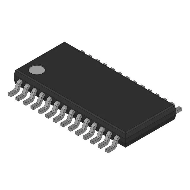
Memory density and bus timing for the BOM line
The CY62256VNLL-70ZC is a 256 Kbit asynchronous SRAM organised as 32 K words by 8 bits, so it replaces a standard 32K x 8 memory socket without a board respin — the parallel interface and 28-pin TSOP I footprint match the JEDEC pinout for this density class. The 70 ns access time sets the read-cycle ceiling: a bus master that toggles the chip enable and output enable at 14 MHz or slower can meet the data-valid window without inserting wait states.
The 28-TSOP I package (0.465" body width, 11.80 mm) is a surface-mount footprint common to 32K x 8 SRAMs — the pin 1 orientation and pitch match the industry-standard TSOP I layout, so a layout already routed for this form factor accepts the part without copper changes. It fits indoor equipment, office peripherals, and telecom line cards that stay above freezing; it is not specified for outdoor enclosures or engine-bay ambient where the junction sees -40°C or 85°C+. The part is marked RoHS non-compliant by the manufacturer. If your BOM requires RoHS exemption or a fully compliant bill, this flag needs a waiver or an alternative finish — the lead-bearing solder balls are compatible with legacy tin-lead assembly lines but not with lead-free reflow profiles that demand pure tin terminations.
The part is not held in ready inventory — lead time is quoted per RFQ.